Continue to Site

Welcome to EDAboard.com

Welcome to our site! EDAboard.com is an international Electronics Discussion Forum focused on EDA software, circuits, schematics, books, theory, papers, asic, pld, 8051, DSP, Network, RF, Analog Design, PCB, Service Manuals... and a whole lot more! To participate you need to register. Registration is free. Click here to register now.

which is the best circuit for photodiode

Status
Not open for further replies.

4tuty

Member level 3
Joined
Mar 27, 2012
Messages
56
Helped
0
Reputation
0
Reaction score
0
Trophy points
1,286
Activity points
1,723
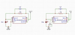
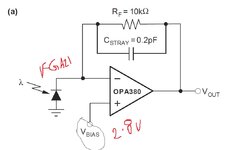
I am going to use FGA21 InGaAs photodiode from thorlabs. I want to know which one of the circuit is better for me (PFA). my application is not for high speed application but i need low noise, linear and precise application.

I saw some tutorial photovoltaic mode is best but from the spec sheet of FGA21 it needs reverse bias of 3V max. so i have used 2.8 V bias for photodiode see figure 2.

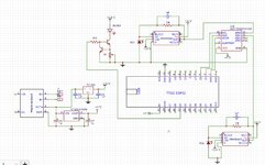
I have used transimpedance amplifier OPA380 for both modes and give the output voltage to ESP 32 A0 pin(not shown). advice needed
 

Attachments

  • PD.jpg
    PD.jpg
    279.5 KB · Views: 364

Hi,

if you want reverse bias, then only fig. 2 satisfies this.
Fig.2 will give far better linearity than the ESP32 ADC. --> Read the ESP32 ADC informations.

OPA380 is fast and it´s expensive. But you don´t need it that fast. I don´t call it Low Noise.
You will get good performance with a low noise CMOS OPAMP .. connected as TIA.

For best performance you need an ADC where you have access to it´s VRef.
Currently you have the VRef of the ADC and VRef for the 2.8V. Both will introduce noise and drift.
With one common VRef you are able to cancel out drifts and reduce noise.

Klaus
 

    4tuty

    Points: 2
    Helpful Answer Positive Rating
Thank you for the reply, I have added the second one to my circuit. for 2.8 volt i used LDO regulator.
OPA380 i bought it :confused:
are my circuit correct? (shall is use MCP602 as opamp)does it needs improvement? i have also attached easyeda files
 

Attachments

  • PD.jpg
    PD.jpg
    576.4 KB · Views: 272
Last edited:

You mention "precision" in your post -

1) The ESP32 not exactly a precision ADC for starters. Looks like its 12 bits
but with error of several bits. And other cautions mentioned in datasheet.


2) The OPA380 not rail to rail, so be aware of that. There are datasheet recommendations
to use an output pulldown to get it to swing to - rail. + rail still not RRIO.

3) The circuit with 5V OPA380 supply will yield higher dynamic range. It also eliminates
the bias accuracy offset which can contribute error if you are trying to achieve absolute
accuracy in photodiode current versus output.

Regards, Dana.
--- Updated ---

The reverse bias spec is a max rating for the diode, not the design
setpoint for the diode.


Regards, Dana.
 
Last edited:

    4tuty

    Points: 2
    Helpful Answer Positive Rating
Hi,

Why are you supplying the amplifiers with 2.8V only? This limits your measurement range and causes unlinearity.

Why is the ADC supplied with 5V, while the ESP32 IO is 3V3 only? Please check compatibility.

I2C signals usually need external pullups

3R3 is to low value.
(Please show name and value of each component. Currently some show nothing, some show name, some show value and some show both)

ADC_ADDR to ESP_GND wiring like in your schematic is no good idea.
You need a solid GND plane. All GNDs need to be connected to this GND plane. (All ESP32_GND, ADC_ADDR, ADC_GND....and all others)

You did non comment about a "common reference". Please confirm that you don´t want to use a common reference.


Klaus
 

You mention "precision" in your post -

1) The ESP32 not exactly a precision ADC for starters. Looks like its 12 bits
but with error of several bits. And other cautions mentioned in datasheet.


2) The OPA380 not rail to rail, so be aware of that. There are datasheet recommendations
to use an output pulldown to get it to swing to - rail. + rail still not RRIO.

3) The circuit with 5V OPA380 supply will yield higher dynamic range. It also eliminates
the bias accuracy offset which can contribute error if you are trying to achieve absolute
accuracy in photodiode current versus output.

Regards, Dana.
--- Updated ---

The reverse bias spec is a max rating for the diode, not the design
setpoint for the diode.


Regards, Dana.

Thank you for the reply. Based on inputs i have made 2 different circuit one with msp602 (as buffer amplifier) another with opa380 with 5V bias input as said both IC's i have now in my hand. Tell me which one shall i go with.

You are correct the 12 bit ADC is not precise so i have added ads1115 which has 16 bit adc.

[The reverse bias spec is a max rating for the diode, not the design
setpoint for the diode.]

yes that is why i used 2.8 volt as reverse bias voltage
 

Attachments

  • PD.jpg
    PD.jpg
    1.1 MB · Views: 178

Hi,

I see you get confused now.
Take a break. Maybe a cup of coffee. Then come back after a a quarter of an hour and read all the posts and the datasheets thoroughly.

****
now to your last post:
i have made 2 different circuit one with msp602 (as buffer amplifier) another with opa380 with 5V bias input
* Why the MSP602 as buffer? No one recommended this. The datasheet includes example ciruits for photodiodes. All are in TIA instead of buffer configuration.
* I see no OPA380 with 2.8V photodiode bias. All have 2.8V bias. One is 5V supplied while the others are still 2.8V supplied.

--> please define your requirements first. Tell us your requirements. Then decide (with our help) a solution.

*****
You are correct the 12 bit ADC is not precise so i have added ads1115 which has 16 bit adc.
It´s not the problem of 12bit vs 16 bit. The problem is that especially the ESP32_ADC is very nonlinear. It is worse than any 8 bit ADC I´ve seen.

--> same as above: first define your requirements. What linearity/accuracy/precision/sample rate/signal bandwidth do you need? Then decide which ADC to choose.
Maybe the ADS1115 is good for your application. I don´t know yet. But it has the drawback of not giving access the it´s VRef.

Klaus
 

Your schematic suggests that you are powering the circuit from a single Li-ion cell (that has a typical voltage of 3.7V approx)- how the 5V regulator work in that case? Please see the minimum input required for this regulator to give 5V.
--- Updated ---

Reverse bias mainly a speed issue, operating with 0 Vdc bias otherwise
acceptable with a TIA, which gets rid of bias errors and noise.
There is a graph for the noise and reverse bias -but I do not see that - but I think the noise decreases with the bias voltage? Or it is the other way?
 
Last edited:

The problems discussed in the thread (noise, speed) are almost irrelevant for the given circuit with slow ADC, 10 ms time constant and low gain.
 

Hi,

I see you get confused now.
Take a break. Maybe a cup of coffee. Then come back after a a quarter of an hour and read all the posts and the datasheets thoroughly.

****
now to your last post:

* Why the MSP602 as buffer? No one recommended this. The datasheet includes example ciruits for photodiodes. All are in TIA instead of buffer configuration.
* I see no OPA380 with 2.8V photodiode bias. All have 2.8V bias. One is 5V supplied while the others are still 2.8V supplied.

--> please define your requirements first. Tell us your requirements. Then decide (with our help) a solution.

*****

It´s not the problem of 12bit vs 16 bit. The problem is that especially the ESP32_ADC is very nonlinear. It is worse than any 8 bit ADC I´ve seen.

--> same as above: first define your requirements. What linearity/accuracy/precision/sample rate/signal bandwidth do you need? Then decide which ADC to choose.
Maybe the ADS1115 is good for your application. I don´t know yet. But it has the drawback of not giving access the it´s VRef.

Klaus


Thanks again for the reply.

I want to measure the skin reflection to detect melanin. I am using IR light and PD. I am not driving the LED using any frequency just on and off with constant current driver circuit enabled from pin 13 (PFA-pg.txt).

1. powering using 3.7 V rechargeable battery and connected to voltage regulator using TP4056 LI-charger and booster module to get 2.8 V and 5 V.
2. switch on and off the IRLED 920 nm using a push button
3. measure the reflected light intensity from skin using photodetector.
4. visualize the voltage value in ttgo display(this board i am using).

*This display is capable of tolerating 5v <- see image.
*Due to non-linearity in inbuilt ADC, i have used 16bit ADC ADS1115 i hope it solves.
*Noise not a problem as i take dark reference (by switch off led) and i will subtract manually.
someone said pull up resistor not necessary for ttgo <- check link. if required please tell me how much value to be connected between 3.3v to SCL & SDA.

My doubts is simple

is my connections are correct in PD (PFA-made a better one). I have used OPA380 circuit given in page no.12 Fig 6.(a) from v-bias i have used 2.8 V (3V is maximum rev. bias voltage).PFA for easy access or do i need to use zero bias.

Future work: i want to control the device using android app using wifi.

I hope, I have corrected all the mistakes in circuit as suggested by members.
--- Updated ---

2. PD bias is 2.8 volt so the voltage swing will between 0 to 2.8 volt. then the voltage output given to esp32 through ADS1115. My question here is, will the ads1115 swings between 0 to 5v even though the PD output swings between 0 to 2.8 volt? if so i have to put a voltage divider before connecting to esp32 as the analog pin can able to tolerate 3.3V.
 

Attachments

  • opa.jpg
    opa.jpg
    64.5 KB · Views: 255
  • PD.jpg
    PD.jpg
    470.4 KB · Views: 189
  • pg.txt
    3.2 KB · Views: 84
Last edited:

Hi,

At first I´d like to correct some misunderstanding:
*Noise not a problem as i take dark reference (by switch off led) and i will subtract manually.
Noise is random frequency, a continous but random up and down. Obviously you can´t calibrate it.
What you describe is called "offset calibration".
***
I miss the requirements given in values with units. It helps us to find the right solution four you. But even more important for you to have a target. Without target you sometimes will loose time with over-engineering things, but on the other hand you will lose performance by ignoring errors.
In my eyes it makes no sense to have a 12bit (0.025% resolution) or 16 bit ADC, while the LED current most probaly drifts by (expected) by 4% within a couple of seconds. The error in LED current is 160 times the resolution of a 12 bit ADC.

When your PCB design is not perfect you may cause a jump of ADC value in the range of several percent every time you switch ON/OFF the IR LED.

What I want to say: you need to focus on the part that causes the biggest error. Improve this part. The ADC and maybe the amplifier will be the least critical.
You may improve ADC and amplifier to perfection, but if the IR diode error is that big, then you gain nothing. Really nothing. It´s just a waste of time.

I don´t want to encourage you. I want you to get very good performance with acceptable effort and cost.
But indeed it does not matter what "I want". You have to decide which way to go. So see my posts just as my personal recommendation.

*****
If I understand correctly: this is the measurement idea:
1) IR LED (ON/OFF)
2) --> fixed lumenous IR intensity on skin
3) --> measure reflection (when IR is ON/OFF)
4) --> calculate some values

***
errors. (numbering as above)
1) thermal drift of LED current, aging of LED, influence of LED current to other analog circuitry
2) distance, stray reflections, stray light, angle, location of skin/sensor ...
3) photodiode linearity, thermal drift, amplifier offset drift, gain drift, reference drift, ADC nonlinearities, ADC offset drift, ADC gain drift, ADC reference drift, influence from other circuitry
4) error in formula/algorithm, resolution and rounding errors, ...

There will be more errors.
I guess 1) and 2) will introduce the biggest errors.

****
I don´t recommend to do all at once. I recommend to work step by step.
From deciding requirements in values and units, power supply, IR_LED current, amplifier, ADC to software...

I almost forgot: you need to decide the mesurement timing. Your analog circuit will need time to settle, the ADC will need time to get stable values.... Thus the correct timing is essential.

Example: A first order filter will need
1 tau to settle to about 35% error
2 tau ... 10 % error
3 tau ... 3% error
4 tau .... 1% error
5 tau ... 0.3% error (equals about an 8 bit ADC resolution)
6 tau ... 0.1% error
7 tau ... 0.03% error (about 12 bit resolution)
and so on (as a rule of thumb)

... most probably you will - or at least you should - dismiss all ADC samples and calculations until you get stable, predictable and useful values.

Klaus

added:
someone said
... isn´t a good way to design. Especially not in times when there is so much nonsense in the internet.
Best is to use reliable informations. In case of "I2C" there is a free document with the I2C specification. This is the most reliable source of information. Every designer should keep on this specifiaction.
To keep it short:
I2C definitely needs pull up resistors. If they already exist: good for you.
The value depends on many things. 4k7 or 3k3 are good values to start.
 
Last edited:
  • Like
Reactions: 4tuty

    4tuty

    Points: 2
    Helpful Answer Positive Rating
Hi,

At first I´d like to correct some misunderstanding:

Noise is random frequency, a continous but random up and down. Obviously you can´t calibrate it.
What you describe is called "offset calibration".
***
I miss the requirements given in values with units. It helps us to find the right solution four you. But even more important for you to have a target. Without target you sometimes will loose time with over-engineering things, but on the other hand you will lose performance by ignoring errors.
In my eyes it makes no sense to have a 12bit (0.025% resolution) or 16 bit ADC, while the LED current most probaly drifts by (expected) by 4% within a couple of seconds. The error in LED current is 160 times the resolution of a 12 bit ADC.

When your PCB design is not perfect you may cause a jump of ADC value in the range of several percent every time you switch ON/OFF the IR LED.

What I want to say: you need to focus on the part that causes the biggest error. Improve this part. The ADC and maybe the amplifier will be the least critical.
You may improve ADC and amplifier to perfection, but if the IR diode error is that big, then you gain nothing. Really nothing. It´s just a waste of time.

I don´t want to encourage you. I want you to get very good performance with acceptable effort and cost.
But indeed it does not matter what "I want". You have to decide which way to go. So see my posts just as my personal recommendation.

*****
If I understand correctly: this is the measurement idea:
1) IR LED (ON/OFF)
2) --> fixed lumenous IR intensity on skin
3) --> measure reflection (when IR is ON/OFF)
4) --> calculate some values

***
errors. (numbering as above)
1) thermal drift of LED current, aging of LED, influence of LED current to other analog circuitry
2) distance, stray reflections, stray light, angle, location of skin/sensor ...
3) photodiode linearity, thermal drift, amplifier offset drift, gain drift, reference drift, ADC nonlinearities, ADC offset drift, ADC gain drift, ADC reference drift, influence from other circuitry
4) error in formula/algorithm, resolution and rounding errors, ...

There will be more errors.
I guess 1) and 2) will introduce the biggest errors.

****
I don´t recommend to do all at once. I recommend to work step by step.
From deciding requirements in values and units, power supply, IR_LED current, amplifier, ADC to software...

I almost forgot: you need to decide the mesurement timing. Your analog circuit will need time to settle, the ADC will need time to get stable values.... Thus the correct timing is essential.

Example: A first order filter will need
1 tau to settle to about 35% error
2 tau ... 10 % error
3 tau ... 3% error
4 tau .... 1% error
5 tau ... 0.3% error (equals about an 8 bit ADC resolution)
6 tau ... 0.1% error
7 tau ... 0.03% error (about 12 bit resolution)
and so on (as a rule of thumb)

... most probably you will - or at least you should - dismiss all ADC samples and calculations until you get stable, predictable and useful values.

Klaus

added:

... isn´t a good way to design. Especially not in times when there is so much nonsense in the internet.
Best is to use reliable informations. In case of "I2C" there is a free document with the I2C specification. This is the most reliable source of information. Every designer should keep on this specifiaction.
To keep it short:
I2C definitely needs pull up resistors. If they already exist: good for you.
The value depends on many things. 4k7 or 3k3 are good values to start.
You are correct that errors play only a very minor role in this application.

This is a measurement of reflectivity and is similar to transmittance.

Because all the measurements are at single frequency, the detector sensitivity correction need to be done at one frequency once only. This is a very important simplification.

The quantity of importance is optical density of the reflectivity- this is proportional to the logarithm of the reflected light.

The physical concentration of melanin in the surface layers of the skin is now linearly related to the optical density of the skin (ignoring other factors).

Most fair skin and most dark skin will differ by OD (optical density) of 2 unit max (in other words, the dark skin reflects 1% of light compared to the white skin)- at that frequency dark skin does not look so dark!

Because we shall be comparing two different samples and there are too many variables, it will be enough if you get about 1% accuracy in the measurement of the reflected light.

an 8-bit ADC would be enough.

Most LEDs are very linear with current; you can have one switch to select a 10x current through the illuminating LED
 
  • Love
Reactions: 4tuty

    4tuty

    Points: 2
    Helpful Answer Positive Rating
Status
Not open for further replies.

Part and Inventory Search

Welcome to EDABoard.com

Sponsor

Back
Top