Continue to Site

Welcome to EDAboard.com

Welcome to our site! EDAboard.com is an international Electronics Discussion Forum focused on EDA software, circuits, schematics, books, theory, papers, asic, pld, 8051, DSP, Network, RF, Analog Design, PCB, Service Manuals... and a whole lot more! To participate you need to register. Registration is free. Click here to register now.

offset voltage in fully differential switched capacitor amplifiers

Status
Not open for further replies.

Chinmaye

Full Member level 3
Joined
Jan 18, 2016
Messages
164
Helped
0
Reputation
0
Reaction score
1
Trophy points
1,298
Activity points
3,145
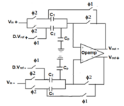
I have designed a flip-around fully differential switched-capacitor multiply-by-2 amplifier. I have seen a few IEEE journals that calibrate the offset voltage of the op-amp. But, I feel the offset voltage is taken care of by the differential structure. I don't understand the need to calibrate the offset voltage of the op-amp. Could someone explain this?
 

Hi,

I can just guess..
You mixed up "common mode voltage" with " offset voltage".

If not, draw a picture of what you mean.

Klaus
 

Hi,

I can just guess..
You mixed up "common mode voltage" with " offset voltage".

If not, draw a picture of what you mean.

Klaus
I am attaching the switched capacitor circuit. By the principle of conservation of charge, the output voltage Vout at the end of amplification phase, is given by
Vout = (C1+C2)/(C1 + (C1+C2+Cp)/A). Vin - D. Vref (C2)/(C1 + (C1+C2+Cp)/A). Vin + (C1+C2+Cp)/(C1 + (C1+C2+Cp)/A)Vos.

But, due to the differential structure, the last term is very negligible, right? A few papers treat this as a significant term. I am trying to understand why?
 

Attachments

  • Fig1.PNG
    Fig1.PNG
    23.2 KB · Views: 180

I don't know, but why do you see it is negligible?
If Cp is small, and (C1+C2+Cp)/A is negligible, then Vos dependent part of Vout is ~(1+C2/C1)*Vos?
I haven't checked your expression, and a bit confusing how it is looking, but I don't see how this part is negligible at all.
 

    Chinmaye

    Points: 2
    Helpful Answer Positive Rating
I don't know, but why do you see it is negligible?
If Cp is small, and (C1+C2+Cp)/A is negligible, then Vos dependent part of Vout is ~(1+C2/C1)*Vos?
I haven't checked your expression, and a bit confusing how it is looking, but I don't see how this part is negligible at all.
The expression was not for a fully differential structure. It was for a single-ended input and single-ended output structure (Half circuit). I feel the last term should ideally cancel for differential structure. The offset voltage might be due to charge injection from the switches and hence shall cancel out during the differential operation. Please let me know if you think otherwise. Thank you
 

I agree differential structure reduces charge injection caused offset, but I don't see it is negligible. It depends on design and requirements. How switches look like, how big accuracy should be maintained, how many stages applied.

Question could be irrelevant after some Monte Carlo mismatch simulation, charge injection is a modeled phenomenon and definitely it will cause some offset, even you are using differential SC circuit, and you should know the offset is acceptable or not for you.
 

    Chinmaye

    Points: 2
    Helpful Answer Positive Rating
Just only because of using differential pair loaded by current sources you have an offset caused by mismatch in these transistor, and it can be in order of tens mV.
 

    Chinmaye

    Points: 2
    Helpful Answer Positive Rating
Differential structure, that is differential amplifier, just by the fact that it's differential doesn't remove the amplifier offset. The differential structure can only help with common-mode charge injection, especially when bottom plate sampling is used as is the case in the flip around S/H. What helps with the amplifier offset in the circuit shown above is that during Phi2 it also performs autozeroing which reduces the offset.
Could you please explain it a little more?
 

I am not sure which part needs more explanation but the amplifier itself has an offset, every amplifier has some. Basically, because of asymmetries when you short together the inputs you get non-zero output. That's basic and it doesn't matter if the OTA is fully differential or single ended.
On the other hand, when you open switches connected to that OTA, they cause charge injection at the inputs buts since this is a balanced fully differential structure, the disturbances caused by the charge injection appear as common-mode signals and are rejected by the amplifier to a certain extend. Since that flip-around topology uses bottom plate sampling, the charge injection at the OTA inputs is pretty much input signal independent which is a good thing.
Lastly, during Phi2 the OTA is connected in a unity gain configuration, so it's offset appears between the inputs of the OTA and on the right side of the sampling caps. On the left side you have the input voltage. Thus caps are charged to the difference between the input and offset. This should cancel the offset in the following redistribution phase Phi1. The higher the gain of the OTA, the better the offset cancellation. I am sure you can analyze the circuit applying charge conservation at the inputs of the amplifier, taking into account also the offset and see how this autozeroing happens.
 

    Chinmaye

    Points: 2
    Always comes to my rescue when I am stuck with any concept. Have learnt many new concepts in this process. I cannot thank you enough
Status
Not open for further replies.

Part and Inventory Search

Welcome to EDABoard.com

Sponsor

Back
Top