Continue to Site

Welcome to EDAboard.com

Welcome to our site! EDAboard.com is an international Electronics Discussion Forum focused on EDA software, circuits, schematics, books, theory, papers, asic, pld, 8051, DSP, Network, RF, Analog Design, PCB, Service Manuals... and a whole lot more! To participate you need to register. Registration is free. Click here to register now.

optimal load resistance for Class AB Power Amplifier

Status
Not open for further replies.

ZionWi1

Newbie
Joined
Feb 23, 2021
Messages
5
Helped
0
Reputation
0
Reaction score
0
Trophy points
1
Activity points
70
Hello all,
I have been studying Class A and Class B power amp., and according to my lecture script R_opt_load_classA&B = (V_max-V_knee)/I_max applies. I can see this in the output characteristic of the transistor:
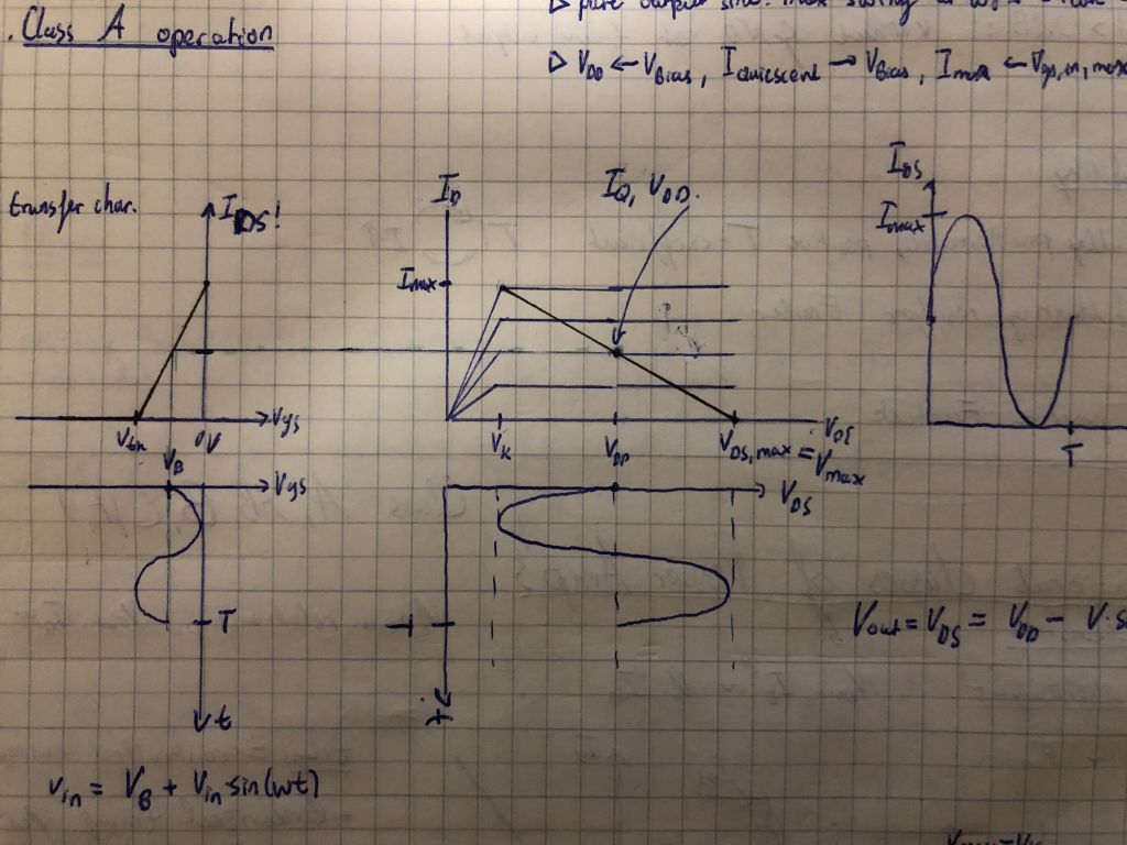
AMP.jpg


Furthermore it is said that the optimal load for Class AB is different: "at Class AB, the Optimum loadline is smaller than R_opt,classA= R_opt,classB". However no formula for an optimal loadline is given. Does a formula for R_opt,classAB depending on the quiescent Current / the conduction angle exist? Or does it need to be determined in a simulation with varying Load resistance?
The circuit of the Power Amp in Class AB operation:
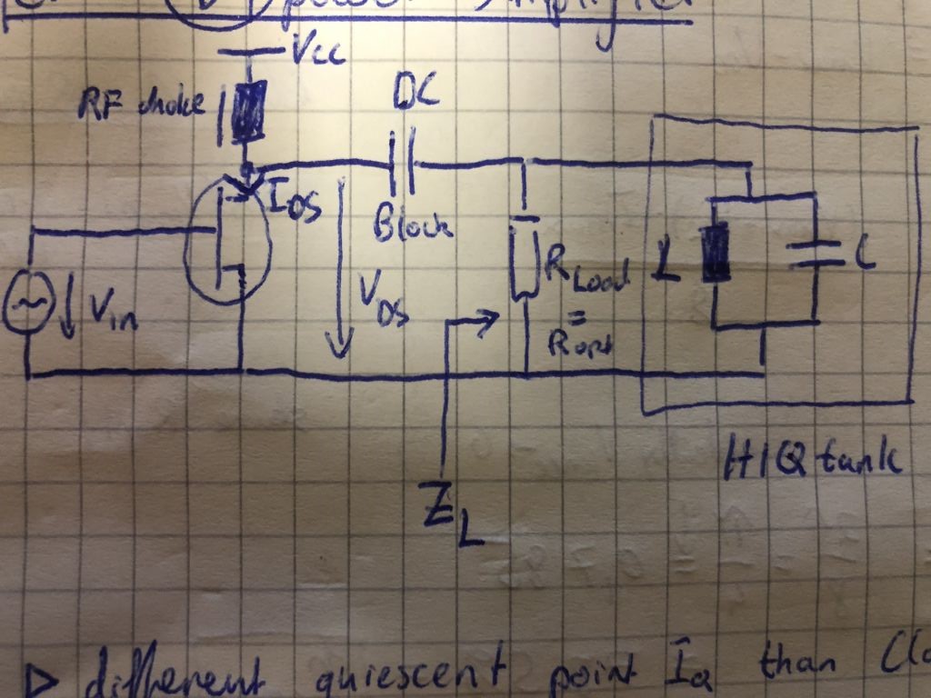
AMP2.jpg
 

Because AB-Class Power Amplifier's operating Point is not defined. It's between \[ 180^o<\theta<360^o \]
Therefore there is no formulae for that.If you shift \[ V_{ds,max} \] to left, you will see this effect.
 

    ZionWi1

    Points: 2
    Helpful Answer Positive Rating
Thanks! So you mean when choosing a quiescent current in the Class AB regime, the fixed point (V_dd, I_q) in the output characteristic I_d (V_ds) moves down (compared to Class A), and when our loadline is supposed to connect (V_knee,I_max) and (V_dd, I_q) we get a steeper load line ~ 1/R, and therfore a smaller resistance?
(refering to " If you shift Vds,max to left")
 

1.- read

[/URL]

2.- Note that while RL just resistive one can built a ‘triangle’ and approximate Rout, then the Load Line impedance just has to be Rout for max power transfer. But the load of the MOSFET circuit closing your question has a capacitor, therefore the load curve to overlap on transistor(s) I(V) is no longer a straight line. The relevant graphs are included in lecture available from above link.

Screenshot_20210226-082240.jpeg


3.- Simulate the circuit with a simulator:

Employers hardly pay any more a dime for pen and paper electronics design work. It's a long distance, why walk if one can drive.

The lecture in link above from Santa Barbara’s Uni uses Keysight simulator ADS
as college/uni student, the chances are that you may qualify to a free software licence, through your learning institution.r
 
  • Like
Reactions: ZionWi1

    ZionWi1

    Points: 2
    Helpful Answer Positive Rating

    c_mitra

    Points: 2
    Helpful Answer Positive Rating
Conduction Angle should be preferred rather than Quiescent Current.At least, terminology is so..
Yes exactly, when you move \[ V_{ds,max} \] to left, Load Impedance will be smaller.
BUT !
However, Load Line Theory is an Simplified Approximation and it diverges in general case from the Reality.Therefore Load Pull Technique has to be absolutely applied.
 
Thanks! But how can then R_opt_load_classB = R_opt_load_classA be explained? As we have said load impedance decreases with decreasing conduction angle in Class AB. What is the relationship between the used load resistance R_load and the impedance we talked about in the output characteristic ? Is the difference that the load impedance applies for the summed up draincurrent of all harmonics and R_load is the loadline for the fundamental?
 
Last edited:

ZionWi1, this is JohnBG2012.

The reason why RLL_A=RLL_B is shown in slides 32 33 of the referred lecture, have a look.

As one can appreciate, for both A and B the triangle is the same, Load purely resisitve only.

It doesn't matter that for A just one transistor pumping current, or for B there are 2 transisitors because when one is pumping the other one is off.

Do not mix Power with impedance for max transfer: the triangle is the same so from load point of view, does it really matter if there's one transistor pumping in? or 2 taking strick turns?

Hope it helps.
 
Last edited:

    ZionWi1

    Points: 2
    Helpful Answer Positive Rating
Dear John,
Thank you for putting in so much work to help me out, I appreciate it! I will have a look at the lecture slides and the simulation tool now.
 

Hi ZionWil this is JohnBG2021. Actually the moderator has accepted all my comments for your question. I have removed slides 32 33, because with the circuit with Id(Vg) graphs it was enough.

Have you noticed that the moderator uses Keysight logo?

I have asked permission for reproduction to Mr Buckwalter and when reproduction is for educational-only, copyright law has exeption:


students couldn't use the internet if copy right rules were applied to educational-only purposes.

Thanks anyway
 

Status
Not open for further replies.

Part and Inventory Search

Welcome to EDABoard.com

Sponsor

Back
Top