Continue to Site

Welcome to EDAboard.com

Welcome to our site! EDAboard.com is an international Electronics Discussion Forum focused on EDA software, circuits, schematics, books, theory, papers, asic, pld, 8051, DSP, Network, RF, Analog Design, PCB, Service Manuals... and a whole lot more! To participate you need to register. Registration is free. Click here to register now.

Small signal analysis neglecting CDG

Status
Not open for further replies.

mirror_pole

Member level 3
Joined
Nov 22, 2020
Messages
56
Helped
0
Reputation
0
Reaction score
2
Trophy points
8
Activity points
554
Hey guys,

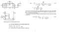
I noticed that often the cap CDG is neglected in small signal analysis. especially if it connects 2 stages of an amplifier. Another example is if i want to calculate the transfer function of a current mirror, lets say the wide swing cascode mirror, i often see that CDG is getting neglected for simplicity.

I know that otherwise the calculation would become pretty complicated, but whats the reason i can neglect this cap? Is it because it is so small that poles or zeros associated with it wont affect the frequency behavior? What about the miller effect though. If i chose a low frequency mirror gain of lets say 10, is it still possible to neglect it ? Also if i apply miller theorem in this case i neglect a zero and the poles are uncoupled so i can assiciate them with nodes, which wont happen if i calculate the whole transfer function.

How accurate is this approximation and where is the limit? Or is it up to me to descide that with simulation results.
 
Last edited:

It is up to you to decide and it is usually the relative importance of the timeconstants coming from different capacitances in the circuit. If you have a circuit in mind, post it here with the values of the caps and the other small signal parameters needed for analysis.
 
hey sutapanaki,

Well im still analysing this flipped voltage follower current mirror and im referring to an analysis which has already been done previous.
Sadly there is no information why they neglect the Gate-Drain caps.
 

Attachments

  • fvf.png
    fvf.png
    105.3 KB · Views: 101

Using signal flow graph analysis makes the problem a lot simpler. That will get
you T(s) quickly, then using PFE you can get to element values.

There are videos on youtube to get you going. I think there are utilities out there
to solve as well. Labview maybe .....?


Cg-d of course matters significantly when looking at input Z and circuits with
a lot of G, eg. Miller effect.


Regards, Dana.

I calculted the transfere functions for \[ Z_{in}(s) \] and The mirror gain \[ H(s)=\frac{I_{out}(s)}{I_{in}(s)} \] with CDG of M2 first (refering to my first post circuit). After the typical self gain approximations i get an extra Zero for H(s) but due to low CDG it is probably at high frequencies. Concerning Zin it also doesnt matter because after approximation compared with the other caps CDG can be neglected. So i understand at least why they neglected this one.

But im not sure about Cdg of Transistor M3 because H(s) gives me a zero but right half plane. I mean its still at high frequencies but could potentionally lead to instability. Also i get a third pole...i know from Miller that this cap will be larger: \[ C_{DG,in}\approx C_{DG}(1-H(0)) \] looking from the input and also \[ C_{DG,out}\approx C_{DG}(1-\frac{1}{H(0)}) \] looking from the output.
My gues was that if lets say \[ H(0)=-\frac{g_{m3}}{g_{m2}}=-1 \] it is still a low cap and can be ignored but im totally not sure about it.

Also thx for the link im gonna dig that.

I mean this cant be the reason because if i look at some OTA topologies they still neglect this caps even with a mirror gain of 5 or even bigger
 
Last edited:

The Cdg of M3 does introduce a RHP zero as is always the case with that cap. The RHP zero by itself doesn't cause instability. It can only be problematic if it appears in a feedback loop. Plus, it also depends how you use this circuit. Since it is effectively a current source, most probably the output current of M3 will go to some low impedance node and in this case you don't care about the Cgd of M3, because it doesn't see a lot of gain. On the pther hand, if the output of M3 goes to a high impedance node, so you provide voltage gain, then yes, the Cgd will be Miller multiplied.
 
The Cdg of M3 does introduce a RHP zero as is always the case with that cap. The RHP zero by itself doesn't cause instability. It can only be problematic if it appears in a feedback loop. Plus, it also depends how you use this circuit. Since it is effectively a current source, most probably the output current of M3 will go to some low impedance node and in this case you don't care about the Cgd of M3, because it doesn't see a lot of gain. On the pther hand, if the output of M3 goes to a high impedance node, so you provide voltage gain, then yes, the Cgd will be Miller multiplied.

I understand. It is actually the same for the simple common source stage. Or maybe in generell if the input is coupled with the output through a capacitance a RHP zero occurs? The cascode stage for example has also the same RHP zero which comes from the cs stage.

About the instability: If i put it in a feedback loop the zero will move to lower frequencies so it has the same influence on phase margin as a LHP pole and therefore the circuit can become unstable?

I didnt fully understand the last part about CGD. This cap connects node n2 (from circuit picture) of the mirror to the output. Do i have to consider the gain Av(0) between the Voltage at n2 and the output Voltage concerning miller multiplication?
So if the output is a high inpedance node, in this case Av(0) will be large and therefore this cap cant be neglected?
 

Every feed forward path from input to output that's in parallel with the main path, will result in a zero. If, however, the main path from input to output, say through a common-source stage is inverting and the feed forward path through the Cgd is non-inverting, then at high frequencies when the feed forward path dominates, it will have the tendency of reversing the polarity of the stage - that is, making it non-inverting, rather than inverting. This is a signature of a RHP zero. So, RHP zero doesn't always occur, only when you have that reversal of polarities.

In a feedback loop the zero doesn't move to lower frequencies. It is where it is, but since it is in the loop it affects the loop gain by decreasing the phase but also not letting the magnitude drop - in a way it hurts you both ways.

There is Cgd from n2 to the output. If your output goes to a load that is relatively high impedance, so you can extract some voltage gain, then the Cgd will see the Miller effect and appear multiplied by the gain at n2. If, instead, the output is treated as current and hence goes to a low impedance load, then you won't have much voltage gain from n2 to the output and consequently not much miller effect for Cgd.
 
thanks! I was not sure about the zero, but i also noticed from calculations of T(s) and closed loop G(s) that the zero never gets affected after applying the feedback, only the poles move closer.

About the feed foward path, actually i read that before but didnt understand it till now.

From my picture CDG is directly connected to the output. So if i actually take a voltage at the output of M3, this would be a high impedance node because of ro,3? But if i only consider the Transfer function of the output current to the input current it wont affect anything in this case?

Lets say i cascode the output, in this case CDG will not be directly connected to the output and. I guess in this case the miller effect will be surpressed by the cascode configuration because of the low impedance node where CDG is connected to (approx 1/gm i think).
 

Got another question, its related to this circuit. I calculated the poles for open and closed loop from the transfer function \[ H(s)=\frac{I_{out}(s)}{I_{in}(s)} \].
In case of open loop i get: \[ p_{d} \approx \frac{1}{C_{2}\left(g_{m1}r_{01}r_{02}\parallel R_{B}\right)} \] and \[ p_{nd}\approx \frac{g_{m1}}{C_{1}} \]. For the dominant pole i can say that its associated with the node n2 because C2 contains all caps from this node to ground and Rout is the resistance gm1ro1ro2||Rb.

In this book for the analysis of this circuit channel lenght modulation is straight up neglected, and im not sure why. I mean if i design the circuit using very large Transistor lenghts, then i kind of understand it but lets say i use sub micrometer lenghts. Doesnt this approximation get quit innacurate? Therefore the dominant pole in their case is just \[ p_{d}\approx \frac{1}{C_{2}R_{B}} \]

If i neglect lambda i can also associate pnd with node n1 since for calculating the resistance M1 is a common gate in parallel with Rs, so resistance is approximatly 1/gm1 but otherwise its "just" a pole.

Now for closed loop:

I got the same expression as in the book, and interestingly for closed loop all output resistances of the transistors dont appear in the approximate transfer function even if i calculate it with \[ \lambda\neq 0 \].
But what i really dont understand is how can i make assumptions whether the poles are real or complex by assuming that the poles already exist :D
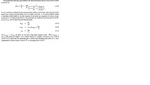
. Its hard to explain and i attach this part with the argumentation. This is the part: For \[ \omega_{OL,nd}>4\omega_{CL,d} \] the poles are real..maybe i just dont get it but dont they already assume the poles in this condition?

Best regards
 

Attachments

  • Unbenannt.png
    Unbenannt.png
    70 KB · Views: 82

Status
Not open for further replies.

Similar threads

Part and Inventory Search

Welcome to EDABoard.com

Sponsor

Back
Top