Continue to Site

Welcome to EDAboard.com

Welcome to our site! EDAboard.com is an international Electronics Discussion Forum focused on EDA software, circuits, schematics, books, theory, papers, asic, pld, 8051, DSP, Network, RF, Analog Design, PCB, Service Manuals... and a whole lot more! To participate you need to register. Registration is free. Click here to register now.

[SOLVED] Negative peak detector Vout incorrect when attached to ZCD circuit. Why?

Status
Not open for further replies.

d123

Advanced Member level 5
Joined
Jun 7, 2015
Messages
2,505
Helped
494
Reputation
992
Reaction score
525
Trophy points
1,393
Location
Spain
Activity points
27,148
Hi,

Just messing around, trying to learn a few things about typical circuits which I think are useful building blocks... I will not be going into mass production with this design, I'm just working through ideas for - and the issues for beginners related to - voltmeter sections. Even so, a little experienced input would be gratefully received as I am perplexed as to the cause of this problem.

I am working on this idea, the circuit here in the schematics, anyone with eyes can see that it is not related to a PSoC, an MCU, a breakout board, a development board or any such thing which has nothing to do with this circuit, please and thank you in advance.

I copied the 'Two-Stage Peak Detector' circuit (page 9, figure 24) from the great Microchip application note attached here and simulated it. It works/simulates (what looks to me) correctly, as can be seen from the schematic and transient results that follow. Positive peak holds at +1V, negative peak holds at -1V.
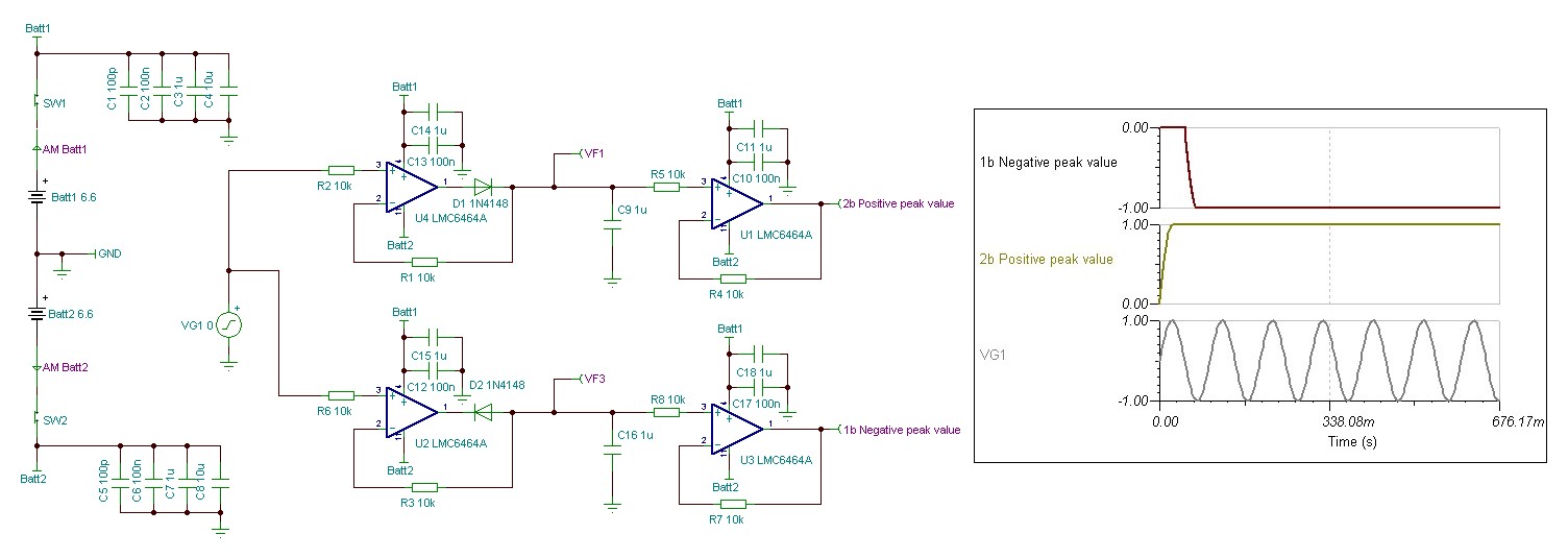
VOLTMETER BUFFER PEAK DETECTOR V1.JPG


When I connect the peak detector circuit to a zero crossing detector circuit - the ZCD is there so as to discharge the peak value capacitors periodically - the negative peak value is no longer reaching -1V, it only goes to ~340mV, as can be seen from the second schematic and transient results below. It does this connected or not to the T1a reset circuitry.
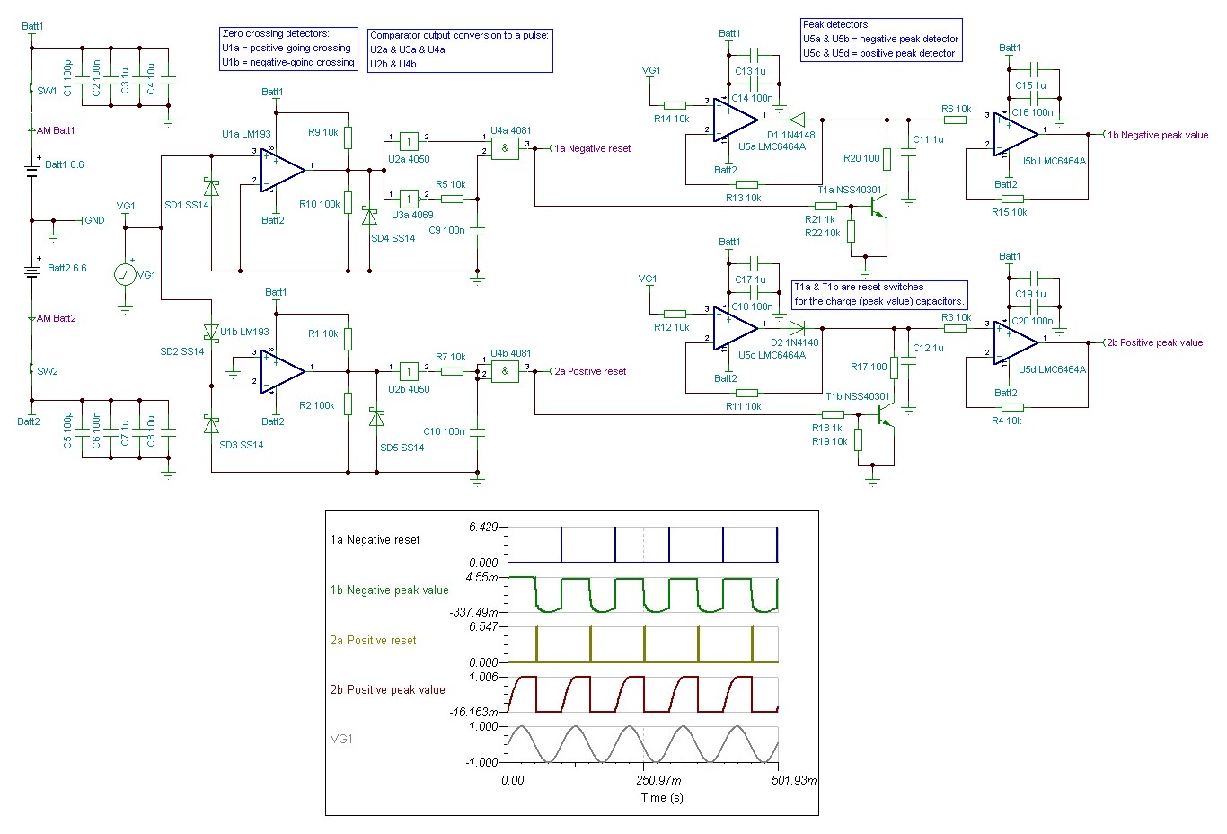
VOLTMETER BUFFER ZCD V1.JPG


I've been messing around with this for a while today (removing things such as the negative reset BJT section, buffering the peak detector inputs, feeling stupid and ignorant, etc.) with no success in recovering the -1Vpeak in = -1Vpeak out signal the negative peak detector produces when not connected to the negative reset/ZCD circuit, and by now I can only dimly understand that it is just some 'newbie' error (of reasoning/design) that I am committing for the negative peak to fall from -1V to -340mV or the simulator has some issue with the ZCD circuit being in the same schematic (I wish - blame the tools, not the idiot). Is this something to do with the simulator or it is actually something about the design?

Can anyone help me see what is incorrect about the negative peak detector section and ZCD and reset circuitry to make it do that, please?

Thanks.
 

Attachments

  • Op Amp Rectifiers Peak Detectors and Clamps AN-1353 Microchip 01353A.pdf
    658.2 KB · Views: 134

no idea
my apologies if i am stating the obvious, or missed it in the text

the positive reset circuit has SD2, where the negative reset does not
U4A and U4B are wired differently

if the negative peak detect is at -1 V when the peak is detected, (plot wthout zero crossing)
the NPN reset transistor (T1a) has its collector at negative voltage -
i do not see how the NPN can pull it down (up?) to 0?
 
  • Like
Reactions: d123

    d123

    Points: 2
    Helpful Answer Positive Rating
I think T1A should be a PNP.
Both transistors might be zapped by reverse emitter-base voltages more than 6V unless they have protection diode circuits.
 
  • Like
Reactions: d123

    d123

    Points: 2
    Helpful Answer Positive Rating
The reset switches are bad designed, particularly for the negative peak detector. The collector base junction will be forward biased by negative signals.

A saturation voltage of -340 mV is however not plausible. It looke like the circuit has hidden connections.

i do not see how the NPN can pull it down (up?) to 0?
It works as a diode switch, without any current gain.
 
  • Like
Reactions: d123

    d123

    Points: 2
    Helpful Answer Positive Rating
Hi wwfeldman,

no idea
my apologies if i am stating the obvious, or missed it in the text

the positive reset circuit has SD2, where the negative reset does not
U4A and U4B are wired differently

I did the ZCD section a couple of years ago, it's a modified copy from bona fide circuits I researched a bit (not copied from a dubious cirkuitz website). The diodes are correctly placed for their purpose: sensing positive and negative going transistions around 0V. I just remember that the logic was a bit of a puzzle to get the short output pulses right and to make them happen at the right times.

if the negative peak detect is at -1 V when the peak is detected, (plot wthout zero crossing)
the NPN reset transistor (T1a) has its collector at negative voltage -
i do not see how the NPN can pull it down (up?) to 0?

That's one thing I was wondering about yesterday but I don't know how to resolve it. The input is on a dual supply, logic is on a single supply, and the NPN would need to be on a dual supply as well or something as the peak detectors are also on a dual supply, I suppose.

__________________________________________________________________________

Hi Audioguru,

I think T1A should be a PNP.

Okay, thanks, I'll try that. I tried that yesterday, besides pointlessly replacing it with a JFET, and I will have another go in that direction today, time permitting.

Both transistors might be zapped by reverse emitter-base voltages more than 6V unless they have protection diode circuits.

I hadn't even thought of that, thank you.

__________________________________________________________________________

Hi FvM,

The reset switches are bad designed, particularly for the negative peak detector. The collector base junction will be forward biased by negative signals.

Okay, thanks. Do you have any suggestions for a better design or a suggestion of what I should read up on? I just can't see a way forward with this (simulation) problem at the moment.


A saturation voltage of -340 mV is however not plausible. It looke like the circuit has hidden connections.

Great, the -340mV is not plausible, good. There's nothing hidden there, that's the whole circuit, I'm not sure what you mean; the logic gates are powered by Batt1. What does 'hidden connections' mean, what should I be looking for?

__________________________________________________________________________

Many thanks for the input and suggestions.
 

Hi,

An even larger schematic..., sorry. I haven't got round to adding the protection diodes yet.

The schematic just shows the added voltage followers and the simulation results, both as separate waveforms and together. It would seem that the issue was related to not buffering the input signal. Even so, the negative peak capacitor doesn't hold it's voltage, it just follows the input signal, basically. Any suggestions on how to get the negative peak capacitor to behave the same as the positive peak capacitor, please? Is the problem related to the NPN - T1a - and the power supply and signal polarities?

VOLTMETER BUFFER ZCD V1B.JPG
 

T1A is an NPN transistor that gets a negative voltage on its collector. Then its collector-base conducts all the time. It should be a PNP but needing a negative base voltage to turn on.
 
  • Like
Reactions: d123

    d123

    Points: 2
    Helpful Answer Positive Rating
The circuit is basically:

Input buffer stages
pulse generators
precision rectifiers
voltage 'reset' clamps
output buffer stages

The positive side is OK as it is, the zero crossing (technically and edge detector rather than ZCD) shoots a pulse into T1a to short the charge in the positive peak capacitor C11.

For the negative peak, duplicate the edge detector, keep T1b as it is but instead of shorting C12, use it to drive a second transistor (PNP) which shorts C12.

Note that simply squaring the input waveform then using an XOR gate with one input delayed will produce a reset pulse for both edges. It may be possible to eliminate the reset pulse altogether and use the 'squared up' input signal to hold C11 & C12 shorted on the half cycle not wanted and allow charging on the wanted polarity.

Brian.
 
As mentioned by others, a npn transistor is a bad choice for the negative reset switch, mainly due to missing current gain and low BE-junction breakdown voltage. Nevertheless, a normal npn transistor won't show the strong leakage current observed in this circuit. Either the transistor has special properties that make it unusable for this circuit or the transistor model is flawed.
 
  • Like
Reactions: d123

    d123

    Points: 2
    Helpful Answer Positive Rating
Hi,

From your kind replies, I'm wondering if 'less is more', and a lot simpler to implement, i.e. removing logic and reset transistors and just using the comparators to reset the charge capacitors, as Brian noted.

The simulator is good but does have some quirks. The NPN is just a dual matched TUN, really, so it can be replaced by other typical TUNs and the circuits work the same. I wonder too as the well-developed-well-defined 2N2222A model is 'perfect' everywhere, this one is glitchy/problematic in some simulations.
 

I suspect partial operation in the simulation is more to do with the C-B junction of the transistor becoming forward biased. Consider that the emitter is at 0V, it is being asked to conduct by making the base positive with respect to the emitter (as normal) but the collector has a negative voltage on it.

Brian.
 
  • Like
Reactions: d123

    d123

    Points: 2
    Helpful Answer Positive Rating
Hi,

Before the circuit I'm working through and its problems: Is there not a far simpler implementation of this requirement/function that uses less parts? 8 op amps and 2 comparators plus three transistors smells of inexperienced circuit-maker/hobbyist (that dirty word) repeating the same circuit block twice out of ignorance. I only want to be able to measure the peak positive and negative voltages (1% or even 5% accuracy up to +-12V would be nice) to process them for RMS measurement. I'd rather process peak voltages, despite their inaccuracies, especially as RMS value extraction is apparently only accurate for undistorted sine and triangle waves and symmetrical square waves, so what I'm doing is worthless rubbish anyway. I wonder how unpredictably distorted and unsymmetrical signals are measured accurately, I guess with SAR ADCs or something.

After trying to understand what members have been saying who have contributed valuable insights regarding the issue, with a few changes, the negative peak section is simulating/working as desired now. I realize I should have spent more time on dual supply circuits over these years, instead of avoiding them where possible, because I have no idea what I'm doing where transistors and negative voltages are concerned or if the protection diodes are incorrectly positioned. To sum up this circuit so far: the simulation does what I want it to at last - whoopee..., but is it a valid circuit? I don't feel too confident about this circuit as I'm not familiar with peak detectors and using negative voltages with transistors, even if 'positive' and 'negative' are relative concepts regarding potential.

So, can someone tell from the simulation results if the circuit is a sane design that could be implemented in the real world?

VOLTMETER BUFFER ZCD V1B_2 NO LOGIC ETC.JPG
 

T1a probably needs to be a PNP transistor, or some sort of mosfet that can handle a volt or so of reverse bias. T1a is probably never fully turning off.
 
Before suggesting a simpler alternative, is it safe to assume the input will be a sine wave centerd on 0V and at a fixed low frequency (< 1KHz)?
Do you want an output that gives you a steady voltage that just tracks the positive and negative extents of the signal or one that drops to zero every cycle as at present?

Hint: I'm thinking along the lines of a sample and hold circuit that 'samples' half way between zero crossings to find the waveform peaks.

Brian.
 

Hi Brian,

Before suggesting a simpler alternative, is it safe to assume the input will be a sine wave centerd on 0V and at a fixed low frequency (< 1KHz)?
Do you want an output that gives you a steady voltage that just tracks the positive and negative extents of the signal or one that drops to zero every cycle as at present?

Hint: I'm thinking along the lines of a sample and hold circuit that 'samples' half way between zero crossings to find the waveform peaks.

Brian.

I wanted to sample the peak values to both know the + or +- peaks and to extract the RMS value from them via an op amp with a selectable divider at the output (0.707, 0.577 and 1). Idea was being able to input sine, triangle and square waves. Frequency - not sure, up to 100kHz would cover most frequencies I tend use in circuits but as a learning tool it's not an issue, 1kHz is a good range. I hadn't thought about the dropping to zero part, what this circuit does seems fine - resets every half-cycle ready for the next peak, but then that's a possible flaw/nuisance as adding out-of-sync signals together to get the peak-to-peak value would need a workaround.

I'd be interested in seeing your idea as I'll learn one or two or quite a few things and it might help to see what I'm doing from a different angle.
 

What I had in mind was not to rectify the signal to find the peak but to use an SAH circuit that sampled at peak point in the waveform then held the voltage until the next peak came along. Instead of getting an output that resets to zero then climbed to peak each cycle as your present design does, you get a stepped voltage that updates on each cycle and stays steady between updates. The problem with this method is you need to find where the peaks are. On a regular sine, triangle or square wave the peak will be one half cycle from zero crossing but it gets more difficult if the waveform is irregular and the peak isn't in the middle. If the frequency is variable, finding the appropriate delay will be a problem unless you can measure the waveform period. A simple MCU with a built in ADC can do what you want.

Your easiest solution is to use a dedicated RMS to DC converting IC like the AD536 because it doesn't care what the waveform looks like.

Brian.
 
  • Like
Reactions: d123

    d123

    Points: 2
    Helpful Answer Positive Rating
Hi Brian,

I just read the AD536 datasheet earlier to swot up a bit before replying - that's a nice device that takes so many problems out of the RMS measurement issue, and the dB output feature is a nice extra. As Klaus often says: 'Why reinvent the wheel?' - especially as my wheel would be very wonky and bulky from everything I'm seeing about such true RMS/peak/average measurement circuits. In a sense, I eat my words from the top as I see here it's do the sums with an MCU or make a table-sized and even then inaccurate circuit depending on the actual waveform shape.

Your suggestion sounds good for undistorted and symmetrical signals, maybe a little complex to implement with a 'still learning about op amps' approach to circuit design options/solutions such as mine still is.
 

Simple sample-n-hold capacitors. One for positive polarity, the other negative. Both referenced to ground.

Notice the capacitors follow amplitude of the waveform as it increases. They don't decline in amplitude until they're discharged periodically (reset) by transistors. NPN is used for positive, PNP for negative. Adjust timeframe as desired to suit your incoming waveform.

The diodes subtract from the incoming amplitude nevertheless I use them to keep things simple. Of course your precision rectifiers are a way to retain accurate measurement.

two sample-n-hold caps one pos one neg w transis resets.png
 
  • Like
Reactions: d123

    d123

    Points: 2
    Helpful Answer Positive Rating
In principle that is how the first schematic works. The diodes being precision rectifiers and the transistors driven by the ZCD circuit.

Brian.
 

Status
Not open for further replies.

Part and Inventory Search

Welcome to EDABoard.com

Sponsor

Back
Top