Continue to Site

Welcome to EDAboard.com

Welcome to our site! EDAboard.com is an international Electronics Discussion Forum focused on EDA software, circuits, schematics, books, theory, papers, asic, pld, 8051, DSP, Network, RF, Analog Design, PCB, Service Manuals... and a whole lot more! To participate you need to register. Registration is free. Click here to register now.

Suggestion for high speed class AB op-amp

Status
Not open for further replies.
Thank you Dominik,

Soon I will verify the simulation and give you feedback regarding your other comments as well,
thank you very much
 

1. Tail current NMOS: Wtot=120µm, Wfinger=5µm, NF=24, L=0.35µm, Id=2.4mA, Vdssat≈335mV, Vgs≈0.8V
2. Input Pair: Wtot=144µm, Wfinger=12µm, NF=12, L=0.35µm, Id=1.2mA, Vdssat≈240mV, Vgs≈0.7V
3. PMOS Current mirror in 1st Stage: Wtot=120µm, Wfinger=10µm, NF=12, L=0.35µm, Id=1.2mA, Vdssat≈0.4V, Vgs≈1.1V
4. NMOS in 2nd stage: Wtot=1000µm, Wfinger=5µm, NF=200, L=0.35µm, Id=20mA, Vdssat≈335mV, Vgs≈0.8V
5. PMOS in 2nd stage Wtot=2000µm, Wfinger=10µm, NF=200, L=0.35µm, Id=20mA, Vdssat≈0.4V, Vgs≈1.1V
In 2nd stage, current might be 5% higher (so Id≈21mA) due to 0.5V higher Vds (with 1.65V common mode and 3.3V supply)
I checked calculations and they seems to be OK (inversion level for input pair is ≈10, NMOS sources ≈24 and PMOS'es ≈35).
With 1.65V provided to OPAMP input, Vds of tail current should be ca 0.9V so it should ensure 0.5V of margin for saturation.

Dear Dominik

Thanks a lot for your reply,
the circuit is working as you expected, it gives DC gain of 55 dB and GBW less than 198 MHz with phase margin 60 degree

1. I am interested on the method you design the circuit, I usuaully use the classical approach like Allen Holberg procedure,
but for you I see you are talking about inversion factor which never been used by classical approaches,

2. did you the L= 0.35 µm because you have very big ratios ? which if be implemented using L = 1 µm might not be possible or the parasatic cap will be a problem

Still I kept the other part of your post for the next discussion
Thank you very much
Best Regards
 

the circuit is working as you expected, it gives DC gain of 55 dB and GBW less than 198 MHz with phase margin 60 degree
So I underestimated gain by factor of 3. Consequences lack of practice. By play with compensation cap and try to add several Ohms nulling resistor 250MHz should be achievable.

1. I am interested on the method you design the circuit, I usuaully use the classical approach like Allen Holberg procedure,
but for you I see you are talking about inversion factor which never been used by classical approaches,
Compact modelling is on table since 80s, EKV paper is 1995, ACM is 1998. For me it is classic as well ;)
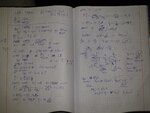
My design notes (calculations were done using gnome calculator)
20200902_205859.jpg

2. did you the L= 0.35 µm because you have very big ratios ? which if be implemented using L = 1 µm might not be possible or the parasatic cap will be a problem
Transit frequency. I see you didn't learn what it is, however I have already blamed you in one thread.
To make any consideration of transfer function, transistors has to operate within desired bandwidth. Signal provided to transistor gate is lost within gate cap if its frequency is higher than ft.
Transit frequency is in first order inversely proportional to channel length and linear with inversion level (current density in channel) - it is not true for decananometer processes, but fit to micron and submicron. For min length 0.35um nmos ft peaking ca 15GHz. For 1um channel it might peak at 1.5GHz (for pmos 0.5GHz), however required VDS might be enormous high and inpractical.
Simply, using transistors which ft is 1GHz does not allows to design amplifier which has more than 100MHz even without any load connected.
 
Last edited:
So I underestimated gain by factor of 3. Consequences lack of practice. By play with compensation cap and try to add several Ohms nulling resistor 250MHz should be achievable.

yes, that is true with this solution,

Compact modelling is on table since 80s, EKV paper is 1995, ACM is 1998. For me it is classic as well ;)
My design notes (calculations were done using gnome calculator)
View attachment 163818


Transit frequency. I see you didn't learn what it is, however I have already blamed you in one thread.
To make any consideration of transfer function, transistors has to operate within desired bandwidth. Signal provided to transistor gate is lost within gate cap if its frequency is higher than ft.
Transit frequency is in first order inversely proportional to channel length and linear with inversion level (current density in channel) - it is not true for decananometer processes, but fit to micron and submicron. For min length 0.35um nmos ft peaking ca 15GHz. For 1um channel it might peak at 1.5GHz (for pmos 0.5GHz), however required VDS might be enormous high and inpractical.
Simply, using transistors which ft is 1GHz does not allows to design amplifier which has more than 100MHz even without any load connected.

Theank you very much Dominik,

I presume you are referring to the gm/ID when you said compact modelling, right? if possible to recommend me good book of it please. and this mean I use the approaches of 60s :) :)

Yes I remember from your past thread when you talked about ft, but I was thinking that with ft = 1 GHz it means I can reach GBW of 1 GHz :)

Usually I use VDS(sat) in the range of 160 mV to 200 mV for speed and headroom consideration.

let me say this is the first time I touch 0.35 µm in analog, I use commonly 0.55 µm as minimum, dont ask me why not 0.5 µm, I just saw it from AMS technology cells,

When I do current mirror with 0.35 µm it looks like a resistor curve, not mirror :)

Anyway your suggested circuit is performing and giving approximately what needed.

I have a question please, and it is very important

I usually design any circuit in the schematic with the number of gate fingers (NG) equal to one, in the time of layout I divide NG according to the matching or size requirements, the result of the layout and schematic are almost identical. In your case you started to divide NG grom the schematic. why?

'Thank you once again
Regards
 

I presume you are referring to the gm/ID when you said compact modelling, right?
Not really. I am using gm/Id curve (1st order) to estimate transconductance for given operating point but not going into all this mnemotechnic flow commonly referred as gm/iD methodology.
if possible to recommend me good book of it please.
What does "good book" mean? I can provide you some titles but I don't know whether such lecture will result with increase your skill/knowledge or only confusion. However, some books which I read, at least:
  1. G. Gindenblat, Compact Modelling. Principles, Techniques and Applications. Springer, 2010.
  2. C. Enz and E. Vittoz, Charge–based MOS Transistor Modeling. The EKV model for low–power and RF IC design. John Willey & Sons Inc., 2006.
  3. P. Jespers, The g m /I D Methodology, a sizing tool for low–voltage analog CMOS Circuits. Springer, 2010.
There is also a book about ACM model (I think written by Galup-Montoro but don't remember now) which might be useful to know as well.
And a lot of papers about EKV, ACM and PSP models available in web. However, you have to be aware about differences in channel charge equations, which might confuse (simply all drain current equations are the same in accuracy to constant which are one time multiplicative, while additive in other time).
One paper which is for sure worth to mention is a work of some Japanese guys, who have presented approach similar to used by myself (I am lazy and usually minimizing my approach so such paper IMO looks not bad with all fancy methodologies):


Yes I remember from your past thread when you talked about ft, but I was thinking that with ft = 1 GHz it means I can reach GBW of 1 GHz :)
It doesn't work like this. Rather imagine that in case of all transistors has 1GHz of f_t, it means that at every node you have pole of 1GHz/number of transistors connected to this net. Some people tried to estimate f_t lower limit for given GBW for amplifiers and they get something like minimum f_t>10×GBW for single stage, >20×UGF for two stage and even higher numbers for multistage architectures.

When I do current mirror with 0.35 µm it looks like a resistor curve, not mirror :)
As I remember this process, it has increase of 10%/1V of drain current. It is really good current source still.

I have a question please, and it is very important

I usually design any circuit in the schematic with the number of gate fingers (NG) equal to one, in the time of layout I divide NG according to the matching or size requirements, the result of the layout and schematic are almost identical. In your case you started to divide NG grom the schematic. why?
Simply, in this process many effects are hidden (because of size, quality of photolitography improved by more than 20 years and modeling - bsim3 doesn't cover many effects).
In simplest words total transistor width is a product of finger width, number of fingers and multiplier factor (number of devices in parallel).
And following relation is conserved (100µm is for example - it is work in general for any):
100µ≠10×10µ≠10×10×1µ
In this technology is possible to see difference between single finger and multifinger wide transistor (effective width is calculated as design width - constant etching number). Simply single finger might have effective width of (let say) 9.8µm instead of 10µm, while with NF=10 and finger design width of 1µm, effective width will be 10×0.8=8µm. And such stuff is covered.

What is not covered (in your process with my best knowledge):
  • WPE - Well Proximity Effect - change in doping (and then in V_Th) due to distance between channel and closest well
  • transistor asymetry caused by 7° deviation from normal of ion implantation - it changes electrical field close to drain region depending to orientation. So, multi finger device behave differently than single finger in parallel
  • Channel stress caused by STI strain, commonly known as LOD (Length of Diffusion). Each finger of multifinger transistor has different threshold voltage. In some technologies, threshold voltage varies even 100mV on the distance betwen edge of diffusion and gate below 1µm.
Above effects are covered by models used in modern technologies. There might be some other effects as well.
Their impact depends to process and in some is visible more, some less.

Basically, this is long story. Also, I don't feel competent to covering this.
 
In order to get accurate filtering for skirts and group delay critical needs, I recall that the GBW needs are exponentially multiplied by the Q of the filter.

Now the best commercial IC's with 4GHz GBW use a combination CMOS front-end buffer, then differential Cascode BJT and BJT complementary common-emitter drivers with special input bias control instead of common-source or CE Darlington stages.

Then compensation is reduced with Av min =10.

Low Input Bias Current: ±3fA Typ. Room Temperaturen 4pA Max at 125°C
Current Noise (100kHz): 7fA/√Hz
Voltage Noise (1MHz): 4.0nV/√Hz
Extremely Low CIN 0.45pF
Rail-to-Rail Output
1599086144000.png
 
Thank you guys for your useful contribution to my post,

I would like to share this paper about the relationship between high DCgain or high GBW, it is excellent transaction explained it with graphs in section II


Indeed what matters us, is the loop gain magnitude at the signal frequency with a certain gain.
 

Dear friends,

I would like to share with you this nice paper, It add simple modification to the two stage op-amp but greatly improves the performance.
Using this technique I could rise the GBW to 250 MHz with the same power budget, with the cost of added capacitor (5 pF) and MOS resistor as you can see from the paper.


Thank you again for your help
 

Has you get faster step response also?
The guy from the link uses HPF to achieve high frequency class AB operation, but this introduces a zero into transfer function.
Any zero within opamp ugf kills it speed.
Notice, they didn't shown small signal response, only large signal and slew rate enhancement.
 
The link doesn't work for me

Hello Suta,

please try this


and let me know if still not working with you

by any way I attached you a picture of the proposed circuit
claasab.PNG

--- Updated ---

Has you get faster step response also?
The guy from the link uses HPF to achieve high frequency class AB operation, but this introduces a zero into transfer function.
Any zero within opamp ugf kills it speed.
Notice, they didn't shown small signal response, only large signal and slew rate enhancement.

I will test this tomorow and I will compare for you the result for both of class A and AB vesrion, indeed I expect that higher GBW should always be faster, and I didn't notice the zero in the transfer function, I will post the results here soon

Thank you
 

indeed I expect that higher GBW should always be faster, and I didn't notice the zero in the transfer function, I will post the results here soon
Check this post

Zero occurs, because for frequencies higher than 1/(2pi Rlarge Cbat) transconductance of output stage is doubled.
 
Last edited:
The zero may screw up the step response only in the case it forms a close pole-zero doublet with a nearby pole. However, Junus is talking here about opamps for the LPF and perhaps he doesn't deal with step signals yet, because the AAF is in front of the sampler.
 
Yes, it is true. And most probably in LPF our dear friend would never see potential effect.
My point is simple, let him to check and notify that higher number in ac does not necessarily mean faster response.
 
Dear friends,

I would say that zero could effect the speed if it is introduced in the region below or near the GBW, I am dealing with this issue in the indirect compensation techniques, an easy way to see the zero effect is by the flat horizontal region introduced in the output magnitude,

In the case of this technique I cant see it, simulation shows no zero effect and the circuit performance is improved (up to my poor knowledge)

I attached you two files based on Dominik ratio design for the op-amp, the first one is the cllass A and the second onme is the class AB of the proposed one, now as Dominik say, we judge better with results and simulation

Both design are simulated with identical setup condition


Please let me know if you have a problem in opening the file
 

Attachments

  • Miller_classA_test.pdf
    214.3 KB · Views: 86
  • Miller_classAB_test.pdf
    211.4 KB · Views: 87

Dear Dominik,

I have two questions related to your previous post,

How you calculated the SR this way ?

Have you seen my files I attached ?
 

The waveforms are unreadable - considering a few ns rise/fall times in linear scale of 20µs is a bit tough.

If you don't see deterioration in small signal step response I can say lucky you! :)
You found compensation cap is reduced from 7 to 5pF, but notice total cap count is increased to 10pF.

I have no idea how to precisely calculate SR in this free-class-AB guy.
For one direction it seems to be classic min(Itail/(Cc+Cgs_out), Iout/(Cload+Cc))so ≈min(2.4mA/10pF≈240V/µs,20mA/25pF≈800V/µs)≈240V/µs.
For other direction, notice Cbat with Cgs of 2nd current source acting as capacitive divider with ratio in your case ca 0.7.
So, large voltage step at the output of 1st stage is directly added with factor of 0.7 to overdrive voltage of output current source boosting it current needed to charge/discharge Cc and Cload.
 
Thank you Dominik,

I would say that obtained slew rate is much more than needed for 5 MHz as you remember, but the this GBW is needed

I am thinking that why didn't you reduce the tail current to the half and doubled instead the differential pair transistors, by this way the GBW will be the same but the slew rate reduced and still more than enough, also using less current will increase the input current mode range,
 

OK. I misunderstood your question. In class-A Slew Rate is always min(Itail/(Cc+Cg_out),Iout/Cout), where Cout is total cap at output node and Cg_out is gate cap of output transistor. So, in this particular case it was mentioned 180V/µs. Despite it was much beyond minimum for LPF response, it was a side effect of UGF requirement.

I am thinking that why didn't you reduce the tail current to the half and doubled instead the differential pair transistors, by this way the GBW will be the same but the slew rate reduced and still more than enough, also using less current will increase the input current mode range,
I don't know the source of such conclusion. Transconductance is proportional to current. You can't get the same gm by doubling W/L and decreasing current. It simply doesn't work like this. For this particular case, you might get ≈6mS so lost by 40% (because of twice lower current). Moreover the capacitance of input stage increases more than twice and ft is dropped as well.

250MHz UGF with 20pF load forces to use high enough current at the output for it transconductance (simply to achieve non-dominant pole at appropriate location ≈500MHz). This, however, adds large cap (≈7pF) to 1st stage output. Such cap move non-dominant pole greatly.
If you do simple math you can get that poles are :
\[ p_d \approx \frac{g_{1}}{k_{out} C_C +C_{gout} + g_1/g_o (C_C+C_{load})} \]
what means that effectively 1st stage seen 10% more cap than Cc only, and
\[ p_{nd} \approx \frac{g_{mout}}{C_{load}(1+C_{gout}/C_{load} + C_{gout}/C_{C}) } \]
So, UGF calculated more precisely is not gm/Cc but rather is shifted by 10% correction in Cc and additional 10% correction in p_nd located at 2×UGF_target. So, with 10mS input stage gm, 6pF Cc, 20pF Cload and 7pF Cgout, UGF is shifted to 220MHz (from planned 250M).

By starting with only Cload and Cc, it might looks that Cc of 1.5pF and gmin of 2.36mS (Id≈280µA) would be enough, but by applying real output stage cap it would result with creepy performance.
Lets look on the numbers then:
\[ p_{nd} \approx \frac{112mS}{20p(1+0.35+4.65)} \approx 150MHz \]
and UGF ≈ 166MHz with low phase margin (guess ≈35°).

This is the main reason of such 2.4mA tail current - Cc has to be at least comparable with Cg_out and then input gm has to be able to drive Cc+correction and keep output pole separated.
 
Last edited:
Dear Dominik,

Thank you very much for your great help,

Indeed I have tried that practically, and prooving exactly your argument,
you asked me how I get the idea of doupling the W/L and reducing halving the current would give the same gm,

it is from the relationship gm (2* ID* K' *W/L)pow 0.5 or you can further have a look on the attached image from Behzad
gmscale.PNG


See fig c and d have the same magnitude,

However, this calculation is not coverin g the parasatic capacitor introduced by larger W/L nor the effect on the fT as you explained
--- Updated ---

So as I said your explanation is practically prooved, I reduced the current with same factor increased the ratio and I got less gm.

I was always follow the design procedure from literature, for example in Holberg, he first start with defining the tail current for the differential pair according to the required Slew rate, then he find the value of the required gm for the GBW based on that current, he never tried to alter the current for adjusting the GBW rather he only play with W/L,,,,,, may be for one reason, the GBW is not as big as 250 MHz.

By the way, I have no concern about the output current as it should be high enough to puch the non dominant poles with less parasatic transistors
 
Last edited:

Status
Not open for further replies.

Part and Inventory Search

Welcome to EDABoard.com

Sponsor

Back
Top