Welcome to our site! EDAboard.com is an international Electronics Discussion Forum focused on EDA software, circuits, schematics, books, theory, papers, asic, pld, 8051, DSP, Network, RF, Analog Design, PCB, Service Manuals... and a whole lot more! To participate you need to register. Registration is free. Click here to register now.
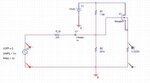
My problem is there seems to be a DC offset of 1.15 volt. Why is that happening. And peek to peak it is 0.5 mV when it should be theoretical 0.884 mV because the voltage gain is 0.884 and the input I am using is 1mV.
The answer in Neamen Ex. 4.7 is 0.884 and I calculated it to be 0.882. But I don't think it should be 0.5 mV
1) Your Mosfet has no part number so we cannot see its spec's.
2) The current is only 0.35mA, it is almost cutoff. Maybe the Mosfet works better at a much higher current.
And peak to peak it is 0.5 mV when it should be theoretical 0.884 mV because the voltage gain is 0.884 and the input I am using is 1mV.
The answer in Neamen Ex. 4.7 is 0.884 and I calculated it to be 0.882. But I don't think it should be 0.5 mV
Did you notice that the example refers to specific transistor parameters Vtn, Kn and \( \lambda \). MBreakN uses quite different default MOSFET parameters. If you set the NMOS model parameters respectively, you can expect similar behavior. Read PSpice manual about MOSFET model parameters.
This site uses cookies to help personalise content, tailor your experience and to keep you logged in if you register.
By continuing to use this site, you are consenting to our use of cookies.