Continue to Site

Welcome to EDAboard.com

Welcome to our site! EDAboard.com is an international Electronics Discussion Forum focused on EDA software, circuits, schematics, books, theory, papers, asic, pld, 8051, DSP, Network, RF, Analog Design, PCB, Service Manuals... and a whole lot more! To participate you need to register. Registration is free. Click here to register now.

[pspice] ERROR -- Convergence problem in transient bias point calculation

Status
Not open for further replies.

renti

Newbie level 6
Joined
Jun 17, 2020
Messages
11
Helped
0
Reputation
0
Reaction score
0
Trophy points
1
Activity points
63
I have read some related posts in this forum, and changed the VNTOL,ABSTOL,ITL1, but it still didn't work yet,
I felt that it was the issure about the GND, the OP, but I don't know what to do .


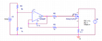
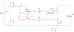
The circuit here is a DC load, which mainly consist of a MOSFET, a shunt resister, an OP amplifier.


When I did the simulation in PSPICS(orcad 9.2), it gave out the following message:
===============================================

** Creating circuit file "test3-schematic1-test3.sim.cir"
** WARNING: THIS AUTOMATICALLY GENERATED FILE MAY BE OVERWRITTEN BY SUBSEQUENT SIMULATIONS

*Libraries:
* Local Libraries :
* From [PSPICE NETLIST] section of C:\Program Files\Orcad\PSpice\PSpice.ini file:
.lib "nom.lib"

*Analysis directives:
.TRAN 0 1000ms 0
.OPTIONS STEPGMIN
.OPTIONS ABSTOL= 1.0n
.OPTIONS ITL1= 500
.OPTIONS ITL4= 100
.OPTIONS VNTOL= 1.0m
.PROBE V(*) I(*) W(*) D(*) NOISE(*)
.INC ".\test3-SCHEMATIC1.net"


**** INCLUDING test3-SCHEMATIC1.net ****
* source TEST3
X_M1A N00413 N00640 N00431 PHN210/PLP
R_R1 0 N00431 0.1
C_C1 N00563 N00685 0.1u
E_U1 N00685 0 VALUE {LIMIT(V(N00966,N00563)*1E6,0V,+12V)}
R_R2 N00685 N00640 10k
V_V3 N01122 0 3Vdc
R_R3 N00563 N00431 1k
R_R4 0 N00966 1k
V_V5 N00413 0 5Vdc
R_R5 N00966 N01122 9k

**** RESUMING test3-schematic1-test3.sim.cir ****
.END

**** 06/17/20 10:19:15 ********* PSpice 9.2 (Mar 2000) ******** ID# 1 ********

** Profile: "SCHEMATIC1-test3" [ E:\1-3 ACimpedance\CircuitDesignSim\mycapturet3\test3-schematic1-test3.sim ]


**** Diode MODEL PARAMETERS


******************************************************************************


X_M1A.Dbody
IS 258.000000E-15
N 1.002
IKF 10.49
BV 30
IBV 10.000000E-06
RS .1773
TT 80.000000E-09
CJO 623.500000E-12
VJ .7055
M .4718


**** 06/17/20 10:19:15 ********* PSpice 9.2 (Mar 2000) ******** ID# 1 ********

** Profile: "SCHEMATIC1-test3" [ E:\1-3 ACimpedance\CircuitDesignSim\mycapturet3\test3-schematic1-test3.sim ]


**** MOSFET MODEL PARAMETERS


******************************************************************************


X_M1A.MOST1 X_M1A.MOST2
NMOS NMOS
LEVEL 3 1
L 2.000000E-06 2.000000E-06
W .54 .54
VTO 2.2 -3.9
KP 20.580000E-06 20.580000E-06
GAMMA 0 0
PHI .6 .6
LAMBDA 0 0
RD .056
RS .02 .02
IS 10.000000E-15 10.000000E-15
JS 0 0
PB .8 .8
PBSW .8 .8
CJ 0 0
CJSW 0 0
CGSO 0 0
CGDO 0 0
CGBO 0 0
TOX 100.000000E-09 0
XJ 0 0
UCRIT 10.000000E+03 10.000000E+03
DIOMOD 1 1
VFB 0 0
LETA 0 0
WETA 0 0
U0 0 0
TEMP 0 0
VDD 0 0
XPART 0 0


ERROR -- Convergence problem in transient bias point calculation


Last node voltages tried were:

NODE VOLTAGE NODE VOLTAGE NODE VOLTAGE NODE VOLTAGE


(N00413) 1.1600 (N00431) .0696 (N00563) .0696 (N00640) 2.7840

(N00685) 2.7840 (N00966) .0696 (N01122) .6960 (X_M1A.4) 1.1600


These devices failed to converge:
E_U1

ERROR -- Discontinuing simulation due to convergence problem
===============================================
 

Attachments

  • 仿真.png
    仿真.png
    30.4 KB · Views: 274
  • 1592361675826.png
    1592361675826.png
    63.7 KB · Views: 224
Last edited by a moderator:

Hi,

I can't see opamp model parameters in your shown log-file.

The error "These devices failed to converge: E_U1" seems to be related with the opamp. Have you included a specific model as for the MOSFET, or is it an ideal opamp. What I'm missing is the power supply of the opamp.

greets
 

    renti

    Points: 2
    Helpful Answer Positive Rating
Hi, stenzer, Thanks a lot! Yes, it worked after I changed the OP model.

The previous model I used was the OPAMP in the ANALOG library, as shown in the picture above, the power supply is set to +12V and 0V in the property editor for the VPOS and VNES respectively.

Now I changed to the model uA741 in the OPAMP library. The circuit worked as expected.

What puzzled me now is that what was the difference between the two OP model?
 

Some more questions.

What this circuit actually wants to do is to test the AC impedance of the power supply source.

Assume that the V_source is the DUT , with the R1 and L1 being its AC impedance.
For a giving frequency of the control signal(V_ctl), the MOSFET(Q1A) will draw a current from the V_source,
then the AC impedance of the V_source at this frequency is obtained by FFT(V_Q1A_D)/ FFT(I_Q1A_D)。

The simulation result at 50Hz and 100Hz seems normal, as there is a slight phase difference between V_Q1A_D with I_Q1A_D, as shown in the picture.
But when the frequency of control signal increased to 150Hz, the result seems terrible.

The sweep frequency required should increase at least to 1K Hz.

My questions are:
1. Is it feasible to test the AC impedance in this way?
2. If yes, which changes should I do to the circuit to improve the response under high frequency?
1592389630134.png

1592389646233.png


1592389727678.png


1592389742657.png
 

Hi,

i assume for such kind of test a sinusoidal waveform is desired. As it seems your are trying to evaluate the overlaying "ripple" voltage.

As the drain voltage is about two times larger than V_source I think your circuitry strats to oscillate in some way. What is the frequency of V(Q1A:d) shown in the last plot? Is it in the range of 500 kHz? It also seems you are using a large time step for your simulation, you may decrease the time step to get a "smoother" result (higher time resulution).

greets
 

Hi, stenzer. Thank you for your reply.

The FFT of V(Q1A:d) in the last plot is as shown. It can be seen that the mainly frequency components are between 1.8k~2.2kHz. And the situation is almost the same when I incresed the frequency to 200Hz, 250Hz, 300Hz,...
1592397966107.png

I wonder If it is feasible in this way to test the AC impedance, and how to avoid the oscillation when I increase the test frequency to at least 1kHz.
 

Please use a smaller timestep for your simulation and upload a reszlt showing a short time instance e.g 10 ms to have a closer look on the simulation result and the waveform.
 

For I am new about pspice, I don't know if the 10ms set in the first plot is the needed setting . and the time-domain of V(Q1A_d) and the FFT are the plots below.
1592402009061.png

1592402099238.png

1592402178939.png
 

Decrease the maximum timestep to e.g. to 1 µs and the run-to-time to ~50 ms. By decreasing the timestep you should get a result with a higher temporal resolution to the cost of a longer simulation time.
 

AC Impedance when the MOS Transistor starts to sink the current from the supply can be found by adding a Current Probe.
Then you can divide and make FFT (VDD/Current Probe). It will give you dynamic AC Impedance.
Don't forget the Phase..
 

Hi, BigBoss. Thank you for your reply. I know the theoretical way to test the AC impedance, but I am not sure If this circuit is a best way to realize it and how to avoid the oscillation when I increase the test frequency to at least 1kHz.
 

Hi, stenzer, I changed the maximum step to 1 us and post the result plot twice here,
The result was quite similar as it was before.
 
Last edited by a moderator:

Status
Not open for further replies.

Part and Inventory Search

Welcome to EDABoard.com

Sponsor

Back
Top