Continue to Site

Welcome to EDAboard.com

Welcome to our site! EDAboard.com is an international Electronics Discussion Forum focused on EDA software, circuits, schematics, books, theory, papers, asic, pld, 8051, DSP, Network, RF, Analog Design, PCB, Service Manuals... and a whole lot more! To participate you need to register. Registration is free. Click here to register now.

Leakage issue in forward converter

Status
Not open for further replies.

mrinalmani

Advanced Member level 1
Joined
Oct 7, 2011
Messages
463
Helped
60
Reputation
121
Reaction score
58
Trophy points
1,318
Location
Delhi, India
Activity points
5,285
Hi
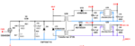
I have a situation where need to use a forward converter. I have never previously worked with forward converters. I am feeling a bit hesitant in using it due to the leakage between the primary bi-filar windings.
Following are the specs:

Input voltage = 60V
output voltage = 12V
Output current = 500mA
Frequency = 300KHz
Input winding inductance = 1000uH (To limit the magnetization current to approx 10% of load)

Even with good coupling between the bifilar winding, with a total of 1000uH there should be at least 5uH of leakage between the bifilar windings itself(guessing). This is enough to spike down the MOSFET.
I have chosen a 100V , 220mOhm MOSFET in SOT23 package. IRLML0100TRPBF
Even with snubbers, I dont see how the effect of a large leakage (5uH) can be suppressed.

Please give some suggestions whether this MOSFET is ok. Also, the MOSFET is being driven by a CMOS 555 timer that can only source and sink 10mA. Will I need a dedicated driver?

Thank you
 

Yes the 555 will drive the mosfet.

Do you have to use a forward converter? 6W is very low power for a forward converter. A flyback controller with a integrated mosfet like a "Top Switch" is made for this type of application.
 
I haven't designed in this particular space but glancing at the mosfet it lists applications as 'load/system switch'. That's not encouraging for a 300khz switching application.

It also strikes me that if you're worried about voltage handling but only have an SOT-23 mosfet there will be many options that solve that problem in packages slightly larger that.

And if space is constrained there should be more integrated options out there than a 555 for control.
 
The leakage inductance example results in < 10 mW snubber losses and shouldn't involve design problems for a RCD circuit. The low Vds rating imposes a low switch duty cycle and tight snubber dimensioning and doesn't sound reasonable.

Although C555 can drive MOSFET gate you'll probably want a dedicated driver to reduce switching losses.

- - - Updated - - -

Forget to mention that the total magnetizing inductance must be reset somehow. If there's no means to recover the energy, it must be absorbed by the snubber, too.
 
I haven't designed in this particular space but glancing at the mosfet it lists applications as 'load/system switch'. That's not encouraging for a 300khz switching application.

I have wondered about wording like this myself in the past. I always look for the data sheet to say OK for SMPS or PWM. Does anyone know how to be sure this device can be used for his 300Khz SMPS.
 

Don't see what qualifies a general purpose MOSFET to be suited for SMPS applications or not. If you manage to design the switcher with sufficient low losses, the SOT-23 transistor should be well possible. You'll notice that complete buck or boost converters with integrated switches are made in similar package sizes.

A different approach would be not to give a damn for 1, 2 or even 4 W losses, just keep the circuit simple.
 
Thanks for the replies.
The development for the complete project (1200VA HF online inverter) is short, nearly 3 months.
The forward converter is a small part of the design and I want to ensure that I get it right the first time. Re-design of PCB just because of the converter can be time consuming, especially in terms of lead time.
I will test the SOT23 FET separately on a different PCB and maybe incorporate it in a later revision. But for the first first main PCB here are a few points:
1. MOSFET = SIB456DK
2. No filter inductor in the output stage. Relying solely on the leakage inductance.
3. A small R in series with the MOSFET. For reduction in current pulse through FET. (output does not have filter inductor)
4. Two groups of RC snubbers. One is connected directly across the FET to arrest package inductance. Other connected across transformer to arrest bi-filar leakage.
5. One 60V TVS across the transformer.
If a few components are not needed, they will be omitted during assembly. But I am providing a footprint for all of the components mentioned above.
Please give some comments on the design. Kindly keep in mind that the design must work in the very first attempt. This is important.
Thank you
 

Attachments

  • Capture.PNG
    Capture.PNG
    28 KB · Views: 189

Transformer windings ratio? Clamping the flyback voltage by D8 doesn't seem well considered.

What's the reason for using a forward instead of a flyback converter?
 

Turn ratio is nearly 1:3 (48V to 16V)
Diode D8 is a 60V TVS operates only when the snubber fails to clamp the spike.
Forward instead of flyback because flyback is inherently more noisy and spiky and thus more prone to faliure and also difficult to get right the first time (probably)
 

Diode D8 is a 60V TVS operates only when the snubber fails to clamp the spike.
How? It looks like you want to reset the transformer inductance through D31. Voltage across D8 and Q3 is then about 96V in flyback phase (for primary 1:1 winding ratio). To limit D8 voltage to 60 V, the duty cycle must be below 25 % and all stored energy is dumped to snubber and D8.

Not to shift the thread topic, I just want to say that I can't agree with the forward versus flyback considerations for the given problem. But instead of starting a theoretical discussion we should look at actual current and voltage waveforms, once you have set up a working forward converter.
 
Thanks for pointing out. I see there is a mistake in the placement of the TVS diode.
I'll revert back after correction.
Thank you
 

Forward instead of flyback because flyback is inherently more noisy and spiky and thus more prone to faliure
Sorry but this is not the case. One transistor forward and flyback, at your low power level, are as noisy as each other.
You are relying on getting a certain value of leakage inductance for it to operate as you want in a forward type fashion, and that’s not easy. It’s a bit “seat of the pants”.
You should be using a flyback converter on all counts. There is no reason to use a one transistor forward which, as you know, needs a demagnitazation winding. Use a flyback and use a primary bias coil to get the secondary regulation….alternatively use a feedback optocoupler or even a simple digital isolator to give you on/off control which is ok for your low power level.
As you know, the demag winding, [ if NP=N(DEMAG)], will put a stress on the fet of 2*vin when it flows current. On top of this you have the leakage spike of the leakage inductance between primary and secondaries…..
At the end of the day, the flyback doesn’t need the demag winding, and still doesnt need an output inductor anyway.
As you declare, the demag winding should preferably be tightly coupled to the primary….but if it is not, then it will still act to demagnetize the core (reset it)…however, it will only be that “bit” of the demag winding that is actually coupled to the primary that does the core demagnetisation. So in effect, if there is leakage inductance there between N(PRI) and N(DEMAG), then it just means it behaves as if you have less turns in your demag winding….which means you get a higher demag current peak ,but lower demag voltage sitting on top of vin.
So anyway, flyback with bias coil is for you….use say a uc3845 (probably cheaper than 555), and shove your feedback signal into it.
 
also i think the lack of source curent sensing in your schem is a bad idea.
What you seem to be setting out to do is perhaps better acieved by a kind of self-oscillating converter that uses the forward type topology.....i think its called a "Royer converter" or something like that......but to be honest, the good old flyback with bias coil is the simplest. I suppose theres the push pull too but why bother when the flyback with bias coil is laying itself bare for you.

http://cds.linear.com/docs/en/application-note/AN118fb.pdf
 
Status
Not open for further replies.

Part and Inventory Search

Welcome to EDABoard.com

Sponsor

Back
Top