Continue to Site

Welcome to EDAboard.com

Welcome to our site! EDAboard.com is an international Electronics Discussion Forum focused on EDA software, circuits, schematics, books, theory, papers, asic, pld, 8051, DSP, Network, RF, Analog Design, PCB, Service Manuals... and a whole lot more! To participate you need to register. Registration is free. Click here to register now.

RF/voltage clamp/limiter

Status
Not open for further replies.

t4_v

Full Member level 2
Joined
Jun 6, 2015
Messages
122
Helped
27
Reputation
54
Reaction score
28
Trophy points
28
Activity points
813
Hi,

I'm looking for a circuit that is called "RF clamp", "RF limiter", "voltage clamp" or "voltage limiter".
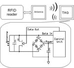
The example of such circuit is a transistor Q on this picture:
j8EGx.jpg

However, what I need is a full RF clamp circuit. Not only the transistor shown in the example above. The gate bias of this transistor would be very useful.

I cannot find many of such circuits. Often, they are stacked diodes on antenna lines or diodes + resistor to bias transistor clamp.

Do you know where I could find good examples? Any books, websites?
 

The circuit has nothing to do with "RF clamp", "RF limiter", "voltage clamp" or "voltage limiter". It's a typical RFID load modulation circuit.
 

A series of shottky diodes in two back to back strings should do it. We used 7+7 (from memory) to protect from 1W, good to 30 MHZ. The secret is to use a ferrite input and output transformer. The DC current saturates the cores giving lower coupling.
Frank
 
@FvM
Right. On this picture the gate of the transistor Q is labeled as "DATA OUT".

However, the same transistor, but with different pin connected to the gate may be used as RF clamp.

I chose this picture as it was the simplest, but I didn't notice "DATA OUT" label.

Here may be a more proper example just to show where RF clamp is located :

https://www.google.pl/imgres?imgurl...P_NAhXCd5oKHQONBbkQMwgiKAQwBA&iact=mrc&uact=8


@chuckey
The problem is I cannot use Schottky diodes. They are no available in CMOS process we use.
 

To get the best circuit efficiency the clamping diodes should be placed outside of the chip. I remember while ago, we were in a situation when the internal CMOS clamping circuit fails very often, due to a poor chip layout design.
 

To get the best circuit efficiency the clamping diodes should be placed outside of the chip. I remember while ago, we were in a situation when the internal CMOS clamping circuit fails very often, due to a poor chip layout design.

You mean back-to-back diodes? You used internally PMOS diode-connected transistors or p-n diodes?

Finally, you took discrete diodes?
 

Status
Not open for further replies.

Similar threads

Part and Inventory Search

Welcome to EDABoard.com

Sponsor

Back
Top