Continue to Site

Welcome to EDAboard.com

Welcome to our site! EDAboard.com is an international Electronics Discussion Forum focused on EDA software, circuits, schematics, books, theory, papers, asic, pld, 8051, DSP, Network, RF, Analog Design, PCB, Service Manuals... and a whole lot more! To participate you need to register. Registration is free. Click here to register now.

How to remove the passivation/IMD/Metal of the Die

Status
Not open for further replies.

junsik

Junior Member level 2
Joined
Feb 17, 2015
Messages
23
Helped
0
Reputation
0
Reaction score
0
Trophy points
1
Activity points
207
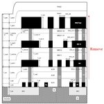
Hi I want to remove the passivation, IMD, metals on the die to take SEM image of the gate.
Please see the figure i uploaded.
How can i remove the passivation, IMDs, and metal lines without the damage on the poly gate of the mosfet??
it is so difficult to find the proper way

Please help me!
thank you
20160527_013848.jpg
 

Any F/A lab knows all of this as their stock in trade,
but a lot of it is not just choice of chemicals but also
time, temperature, agitation and so on, with some
dependence on the process which will lead to some
cut-and-try deprocessing.

If you're looking for a top view you don't really have
to worry about poly damage until the last (Py-M1)
ILD layer removal. This will probably be an HF dip
and can chew silicon, although not as fast as the
oxide.

This is something that, if you have a budget and
not an in-house lab with skilled technician, would best
be sent out to a lab that's capable.
 
  • Like
Reactions: junsik

    junsik

    Points: 2
    Helpful Answer Positive Rating
Dear junsik,

I will try to be brief and clear.

The pasivation can be eliminated via a controled RIE plasma etching (https://en.wikipedia.org/wiki/Reactive-ion_etching). This process is only accesible to clean room technicians.

The Aluminium and Tungsten used for the metal and via levels respectively can be eliminated with a (H2SO4 + H2O) wet etching process. For a standar technology it can take about 4 hours to reach the polysilicon level.

The SiO2 volume can be removed using a HF tamped disolution. The HF acid is extremelly dangerous and should not be used out of the clean room. In 1 hour you should reach the polysilicon layer.

As you can see, the etching process should be performed by clean room technicians.

Greetings.
 
  • Like
Reactions: junsik

    junsik

    Points: 2
    Helpful Answer Positive Rating
A more controlled method is to polish off the layers. All FA labs have specially designed polishers for this, but this can be done using a modified CNC system.
The top nitride layer is most difficult.
This technique allows you to stop at eack metal then via layer. When the last metal layer (metal 1) is removed, the first dielectric layer is removed with buffered HF which also floats off the contact plugs leaving the poly and active layers exposed. This technique will destroy titanium silicide but poly will be intact.
 
  • Like
Reactions: junsik

    junsik

    Points: 2
    Helpful Answer Positive Rating
Status
Not open for further replies.

Part and Inventory Search

Welcome to EDABoard.com

Sponsor

Back
Top