Welcome to our site! EDAboard.com is an international Electronics Discussion Forum focused on EDA software, circuits, schematics, books, theory, papers, asic, pld, 8051, DSP, Network, RF, Analog Design, PCB, Service Manuals... and a whole lot more! To participate you need to register. Registration is free. Click here to register now.
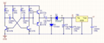
You mean the Q1/Q2 pair? Almost certainly to increase power, to isolate the oscillator section from charge pumping / regulation circuitry behind it. If it happens to invert or not wouldn't make any difference to function here.
Almost certainly to increase power, to isolate the oscillator section from charge pumping / regulation circuitry behind it. If it happens to invert or not wouldn't make any difference to function here.
Could you explain why increase power here?
I have another question hope you could suggest some ideas.
From the circuit above why don't we take the differential voltage from two branches of oscillator into the charge pump?
Possibly the oscillator section (Q3/Q4) would be too 'weak' to drive the capacitor/diode section directly. Or able to "sink" enough current (current from its output -> negative supply), but not "source" enough current (current from positive supply -> its output).
Or (at least as likely) able to do so, but doing so would influence the oscillator section too much. Change frequency, make startup unreliable, whatever.
Why? You only need one output that lets current flow into or out of the diode section (through C7). If that generates the desired voltage, job done. The other 'output' you are suggesting, consists of the "GND" supply line here.
Q1 and Q2 are emitter-followers that have a low input current but a high output current. Emitter-followers are not inverters. Q1 pulls its emitter high with lots of current to charge C7 then Q2 pulls its emitter low to add the charge on C7 to C8 also adding almost the 24V supply. Therefore I think C8 will charge to almost -44V, not -22V. This high voltage will probably destroy the -5V regulator.
This site uses cookies to help personalise content, tailor your experience and to keep you logged in if you register.
By continuing to use this site, you are consenting to our use of cookies.
")