Welcome to our site! EDAboard.com is an international Electronics Discussion Forum focused on EDA software, circuits, schematics, books, theory, papers, asic, pld, 8051, DSP, Network, RF, Analog Design, PCB, Service Manuals... and a whole lot more! To participate you need to register. Registration is free. Click here to register now.
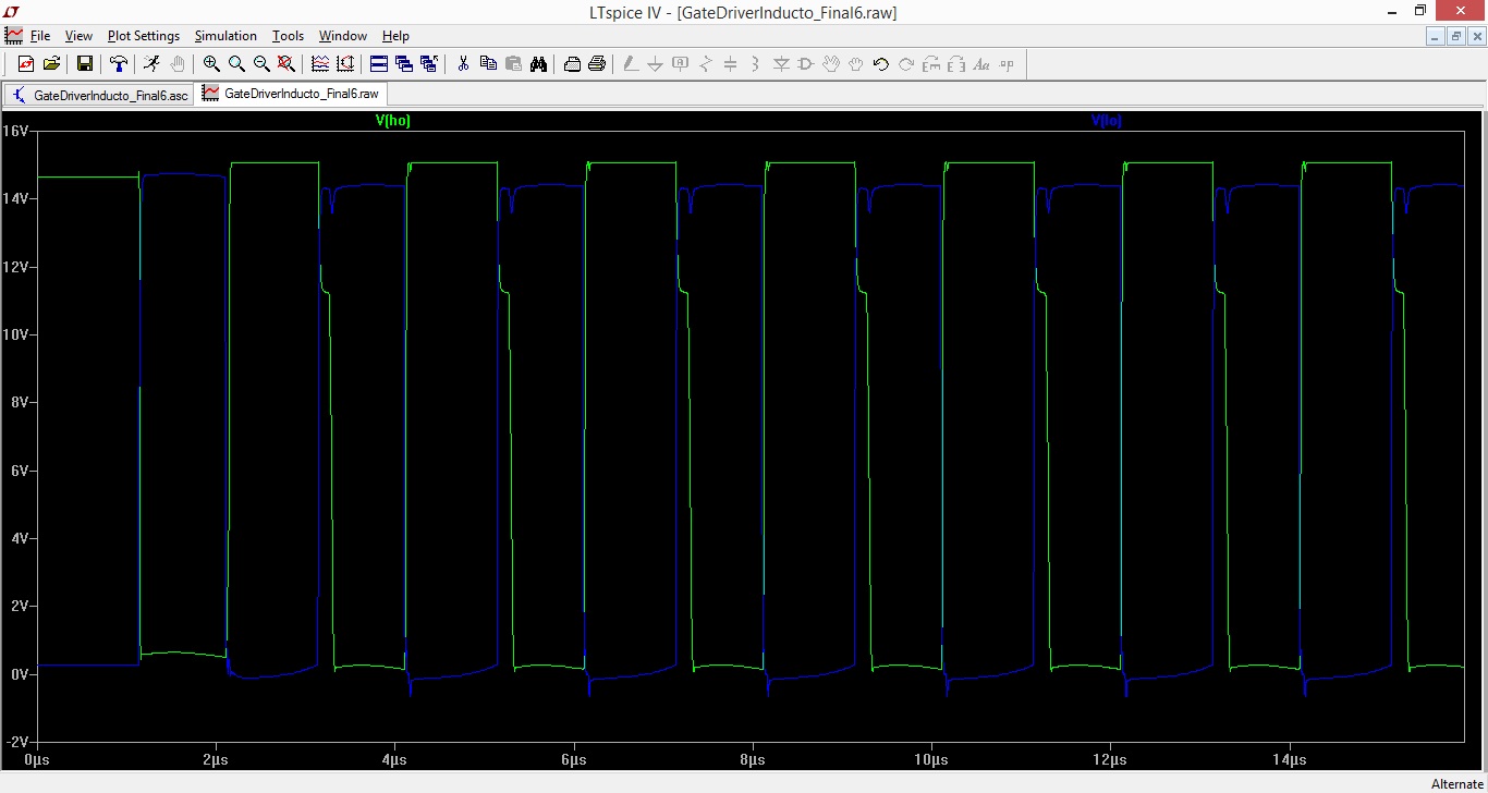
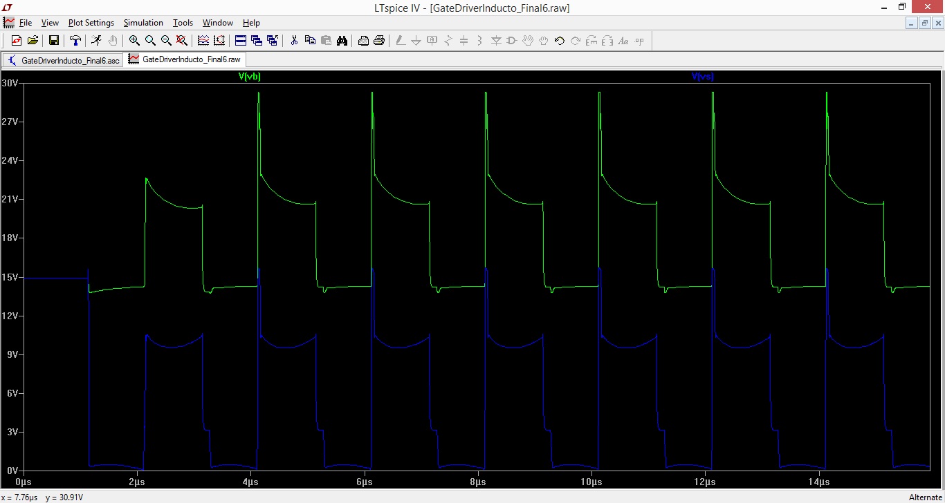
Actually your physical setup is a bit too open (widely spaced) to give you very good results - as seen in your 1MHZ operation screen shot... but things are very well matched at 500kHz (quite by accident) you can tell by looking at the gate drive signals.
Really you need to progress to a multi layer pcb and SMD parts for best performance in the 1MHz arena, proper de-coupling becomes vital and electro's don't really cut it, unless you operate near their self resonant frequency...
I had to stop working on this project for a time but I am back on it again !
I was thinking on using the services of a company, as pcbway.com, to do the prototyping for me. I don't think my skills will enable me to produce a decent work with smd parts.
I read a few things concerning the de-coupling... How do you advise to organize the layout ?
you still have to lay out the pcb before you hand the file over for them to make the blank board and then put the parts on it for you...
Layout = short traces (tracks) & wide for HF & hi power, ground plane underneath control, short loops using power ground (or V+) returns to keep loops short, lots of decoupling near the fets, and on any IC or gate drive circuit, i.e. everywhere...
I am trying to optimize the design before getting to the PCB design.
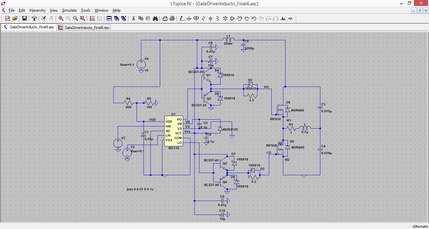
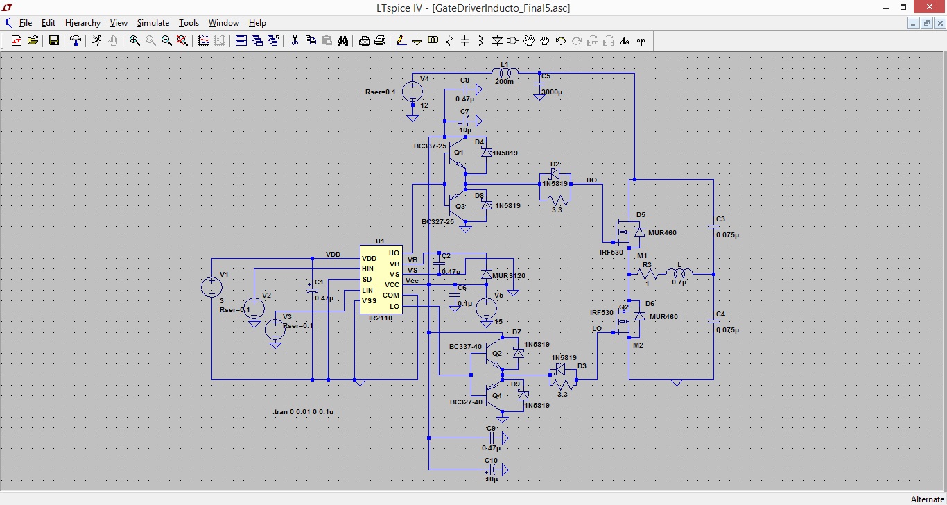
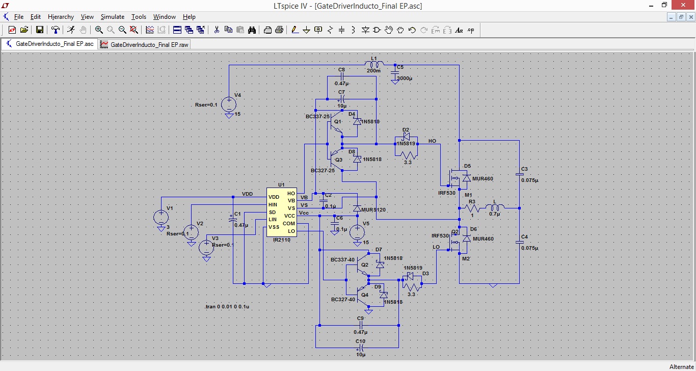
There is various voltage source and I reduced there number.
V2 and V3 are signal from the microcontroller.
But V1 and V5 are connected to the gate driver and the totem pole (for V5). I modified the design in order to have only one voltage source...Does it make sense to have the same voltage source for the power rail and the gate driver signal ? The LTspice are giving exactly the same results. I was just wondering if in a real world pcb that would cause trouble. Should I add a level to protect the IR2110
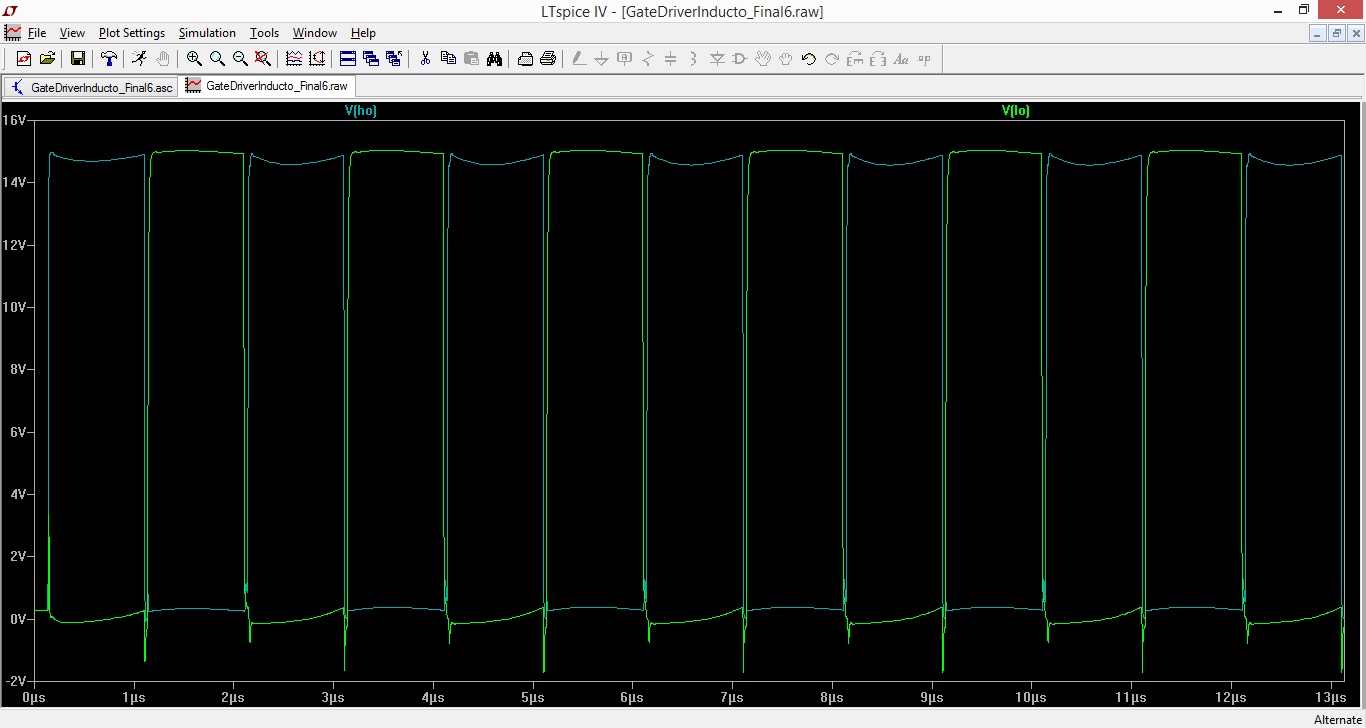
Moreover, I have an issue between my LTspice simulation and the real life experience that I did. I realized, during the experiement, that when Vs was connected to the inductive charge, it gave way better. Than when I put Vs to ground, as per my simulation. But on my LTspice simulation, the results are opposite, better Vs is on ground. When Vs is connected to the charge, there is an overlap between HO and LO if C2 value is high enough. If C2 is lower, HO doesn't maintain at high level for the whole period. Any clue what might be happenning with the simulation ?
The high power ground should be connected together. The gate driver common nodes should connected together. And then, connected together.
But I didn't expect that It would have an impact on the sim.
On the real life pcb, no problem, i knew.
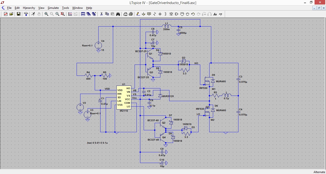
Look at all the points you have shorted together on your sim with your little gnd symbols and ask your self if that was a good idea? A sim can only follow your input, if you short the o/p to gnd - what will you see? is the sim supposed to magically pick up your mistakes?
Q3 collector, C7, C8 do NOT go to gnd, wiring errors on your sim...!
- - - Updated - - -
R5 not needed, R4 should be 10 ohm
- - - Updated - - -
VB should go to collector Q1, you have an extra wire connecting C5 to C7,8 take it out. Also the wire going up from Vcc needs deleting, these are all basic errors easily observable by you simply taking the time to look at your sim circuit...
- - - Updated - - -
Oh in case you missed it collector Q3 goes to Vs...
I am not sure Q3 collector should be connected to Vs. Results are more convicing if It remains on gnd.
Plus, we talked on this post with Orson Cart, how C7, C8, C9 and C10, he advised that he should be on gnd and not on the line.
I did an experimentation and it worked.
You are right to say that Q1 collector should be on Vb and not Vcc as I thought.
I did put C9, C10 on gnd. But results are still not convincing.
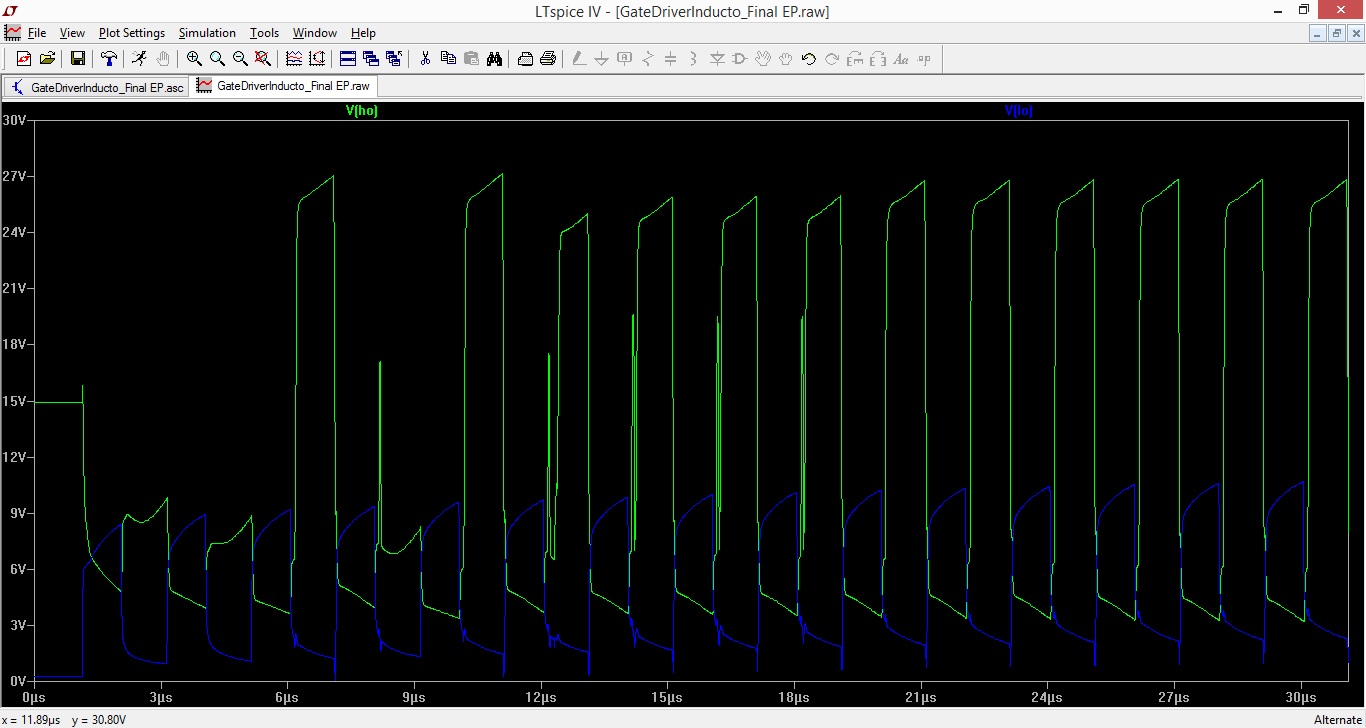
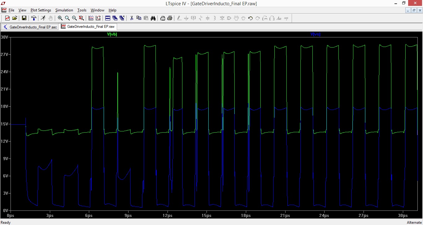
If I increase the power rail volltage, it increases HO voltage as well (to the same level). Which is weird, since they are not correlated.
Thanks a lot for the time
This site uses cookies to help personalise content, tailor your experience and to keep you logged in if you register.
By continuing to use this site, you are consenting to our use of cookies.