Continue to Site

Welcome to EDAboard.com

Welcome to our site! EDAboard.com is an international Electronics Discussion Forum focused on EDA software, circuits, schematics, books, theory, papers, asic, pld, 8051, DSP, Network, RF, Analog Design, PCB, Service Manuals... and a whole lot more! To participate you need to register. Registration is free. Click here to register now.

[SOLVED] Ringing in the edges of a quare wave

Status
Not open for further replies.
What is the frequency of oscillation?
What is the length of the wires on your breadboard?

Numbers always help discussions, since they rule possibilities out.


In which case I assume you are using a *1 probe, which will have ~150pF capacitance (i.e. "C")

What is the inductance associated with the wires (i.e. "L")? (Assume 1nH/mm)

What would you expect the resonant frequency of the LC circuit to be? (Use google if you don't know the formula)

- - - Updated - - -


If you don't want to see what is happening in your implementation, then add the filters.
The probe I am using has a little switch X1 and X10. I am using it on x10.

But there are no other adjustments. Look it was clearly not a top of line probe.

I have used matrix board not PCB. I have created perhaps half the traces on the underside with stripped and tinned magnet wire. The other half are insulated hookup wires on top of the board. It is not exceptionally well optimized for trace length but I kept them to a minimum as much as was practical. So I can't expect to have a pristine square waves etc. But then again I probably can't expect to accurately detect every bit ringing and other signal distortions with a very old style valve based oscilloscope. But my circuit is not a low power precision one, so it probably does not matter.

I am getting to know Ultiboard and am toying with the idea of producing a PCB version of my circuit. Just to try the process out.

I wonder how practical it would be to transfer the printed circuit to a plain fibre glass board (no copper), paint the traces with araldite or something, coat the uncured araldite with Al powder and then plate the traces with copper from slightly acidic copper sulfate. It might be worth a try.

It would certainly be a more efficient use of copper given that copper ore is becoming scarce and copper more expensive.
 

The probe I am using has a little switch X1 and X10. I am using it on x10.

But there are no other adjustments. Look it was clearly not a top of line probe.

Any 10:1 passive probe has at least one adjustment, necessary due to the fact that oscillsocopes have different input capacitance. It may be the case that just didn't find it. What's the fabricate and type?

But wrong adjustment doesn't cause ringing, only overshoot or undershoot with lower frequency (kHz range) pulses as shown below. In so far the point isn't directly related to the thread topic.


Regarding ringing, you already revealed that it's apparently brought up by insufficient power supply bypassing, which sounds plausible to me. Sounds like the thread should be marked as solved.

I got the impression from audio that he didn't think that lack of power supply bypass caps would cause any ringing but perhaps I misinterpreted what he was saying.

I just looked at my probe and it does have a little screw in a plastic rectangular thing adjacent to the BNC connector. I had assumed that was just to hold the casing together.

I can't see any adjustments at the probe end other than the x1 / x10 switch.
 

A 'scope probe that attenuates 10 to 1 uses a trimmer compensation capacitor so that the attenuating resistors attenuate low frequencies and the trimmer cap plus the cable capacitance attenuates high frequencies the same amount. If the trimmer cap capacitance is too low then the high frequencies are cut too much by the cable capacitance. If the trimmer cap capacitance is too high then high frequencies such as the leading and trailing edges of a square wave are not attenuated enough and they are boosted compared to lower frequencies.
 

I just looked at my probe and it does have a little screw in a plastic rectangular thing adjacent to the BNC connector. I had assumed that was just to hold the casing together.

You actually found the adjustment screw. Presume that it produces the waveforms shown in my previous post when driven with a 1 kHz square wave.
 

I got the impression from audio that he didn't think that lack of power supply bypass caps would cause any ringing but perhaps I misinterpreted what he was saying.
I said that the ringing was probably caused because the very important supply bypass caps were missing (because then the wires from the power supply are series inductors and you do not want the circuit powered through inductors).
ALL circuits need power supply bypass capacitors (of the correct value because electrolytic caps have some series inductance) mounted very close (short wires) to the circuits being powered. Many digital circuits use a supply bypass capacitor at each logic IC.

I just looked at my probe and it does have a little screw in a plastic rectangular thing adjacent to the BNC connector. I had assumed that was just to hold the casing together.
I can't see any adjustments at the probe end other than the x1 / x10 switch.
The screw adjusts the compensation trimmer capacitor for the x10 setting.
 

I said that the ringing was probably caused because the very important supply bypass caps were missing (because then the wires from the power supply are series inductors and you do not want the circuit powered through inductors).
ALL circuits need power supply bypass capacitors (of the correct value because electrolytic caps have some series inductance) mounted very close (short wires) to the circuits being powered. Many digital circuits use a supply bypass capacitor at each logic IC.


The screw adjusts the compensation trimmer capacitor for the x10 setting.

So would you regard it as worth while to add any further bypass caps for the logic chips I have used? I have not checked the data sheet for the AND gates etc to see what they require. I suppose if any are the same value as for the 555 then I wouldn't need them.
 

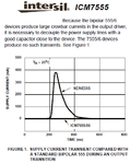
The 555 was designed with old high power TTL technology. Each TTL logic IC needed its own supply bypass capacitor (ceramic 0.01uF or 0.1uF). I forgot to tell you that the output of TTL or a 555 produces a power supply current spike of 400mA each time it switches and the bypass capacitor supplies the peak current if it is close enough. In addition to ringing, without the bypass capacitor the supply voltage to the entire circuit might drop very low for the switching time if there is no bypass capacitor.
More modern CD4xxx Cmos logic ICs are extremely low power and one bypass capacitor is good for a few of them if they are all close together on a pcb. Since you are using a solderless breadboard with fairly long inductive connecting and power supply wires all over the place then you probably need a bypass capacitor for each IC.
 

Attachments

  • 555 supply current spike.PNG
    555 supply current spike.PNG
    27.4 KB · Views: 78

So would you regard it as worth while to add any further bypass caps for the logic chips I have used? I have not checked the data sheet for the AND gates etc to see what they require. I suppose if any are the same value as for the 555 then I wouldn't need them.

Once again, this time for the last time, "What is the frequency of the oscillation? How long are the wires?"

If you can't be bothered to answer simple important questions, and can't be bothered to read/understand the references various people have given you, why do you think we will continue to spend time trying to help you? If you don't know how to measure the frequency, tell us the time period and we'll work it out for ourselves!
 

Re: Ringing in the edges of a SQUARE wave

Is there any point in having a go at adding the filters detailed here: https://lmgtfy.com/?q=how+to+compensate+scope+probe?

Perhaps connect the probe to the scope through a small circuit board where I can solder in the filters. The low frequency filter would be at the wrong end, but perhaps better than nothing?

Or perhaps even use the hook thing on the end of my probe to attach it to a small circuit board with the low frequency filter a sewing needle or something as the new probe soldered to the circuit board? Then the low frequency filter would be at the correct end of the probe.

NO point on all counts.

Read my correct answer again.


edit
Ringing can ONLY occur from a 2nd order effect such as L & C or higher order. L is your cable or ground return wire on the scope or layout poor grounding and decoupling.
C is the probe or load capacitance.

Simple test... calibrate probe on 1kHZ test square wave on scope then try 1MHz square wave on CMOS and repeat.

Use coaxial probe tip and barrel only for best results and not the ground strap.
Once your measurement methods are clean, then reduce the Q of your LC load with a termination resistor to match the cable impedance and DC voltage. e.g. if 5V logic on 120 Ohm twisted pair, the average voltage DC is 2.5V so terminate with two 250 Ohm R, one to +5 one to Gnd. to get 120 OHm termination. If your driver on CMOS is a buffer, chances are it may have an ESR from 50 to 200 Ohms. If this load is too much double the R values and see if your Q resonance or ringing is reduced to ideal Q=0.7 or critically dampened.

RLC nomographs make this an easy job to know what the Q is.
 

No point on all counts.
Read my correct answer again.

His answer (omitted due to this forum's inane policy of only allowing a single level of quoting) is wrong.

But your answer may or may not be right depending on the oscillation frequency and length of "transmission lines". Personally I strongly suspect your answer is wrong in this case, and that the oscillation is determined by a simple LC resonant circuit. Of course, we'll never know if the OP can't be bothered to tell us the frequency.
 

Of course, we'll never know if the OP can't be bothered to tell us the frequency.
On the first post of this thread and on some of his many other threads about this project he said the frequency is 100kHz. When I told him that the lousy old LM324 does not work at frequencies that high then he replaced it with a 555 as a buffer. He said that most of the ringing stopped when he added the supply bypass capacitors that I recommended that were missing on his schematic. Any remaining ringing might be caused by inductive wires all over the place on his solderless breadboard.
 

On the first post of this thread and on some of his many other threads about this project he said the frequency is 100kHz. When I told him that the lousy old LM324 does not work at frequencies that high then he replaced it with a 555 as a buffer. He said that most of the ringing stopped when he added the supply bypass capacitors that I recommended that were missing on his schematic. Any remaining ringing might be caused by inductive wires all over the place on his solderless breadboard.

I read the 100kHz as being part of the desired signal.

If it is the ringing frequency, then my suspisions were correct: scope probe calibration is irrelevant, scope probe ground lead length is irrelevant, whereas lead inductance and layout are dominant. Yet again people spend more time debugging their bl**dy breadboards than debugging their circuit.
 

If the edges of the 100kHz squarewave are ringing then the ringing frequency is probably smack in the middle of the AM broadcast band (1MHz).
A little inductance from the breadboard connecting wires all over the place resonating with the fairly high capacitance between all the rows of contacts on the breadboard.
 

First you calibrate your probe with the 1KHz wave on the scope.
Second you decouple ringing on SUpply with RF caps and/or low ESR tantalum or low ESR Alum caps.
Third you clean up your driver with a proper 50 Ohm CMOS buffer driver or a high current buffer with a small series resistor to drive your 50 or 120 Ohm cable. THen terminate the square wave with the same impedance understanding you lose half the voltage on matched spectral transmission lines for a perfect

Scope probe long 6 in grounds are not irrelevant. they are useless unless looking at low frequency DC or sine waves.
 

His answer (omitted due to this forum's inane policy of only allowing a single level of quoting) is wrong.

But your answer may or may not be right depending on the oscillation frequency and length of "transmission lines". Personally I strongly suspect your answer is wrong in this case, and that the oscillation is determined by a simple LC resonant circuit. Of course, we'll never know if the OP can't be bothered to tell us the frequency.

20kHz square wave as an interrupter for a 80kHz or so square wave.
 

Scope probe long 6 in grounds are not irrelevant. they are useless unless looking at low frequency DC or sine waves.

I am extremely well aware of that, first having experienced the problem in 1976. See https://entertaininghacks.wordpress.com/2015/04/23/scope-probe-accessory-improves-signal-fidelity/ for a good homebrew way of reducing the problem.

Note, however that such resonance will occur at ~100MHz whereas some say that the OP's edges are ringing is at 100kHz. However, since the OP has never posted a picture of the scope trace and remains unable to tell us the frequency of the "ringing in the edges of a quare wave", we will never be sure.
 

Since the OP did not give any details I assumed the worst case which is a x1 probe which has a much lower resonance with a 12" ground clip. BUt you are correct to assume 100KHz must be the ground and signal impedance of the load which has 2nd order LC resonance.
 

On the first post of this thread and on some of his many other threads about this project he said the frequency is 100kHz. When I told him that the lousy old LM324 does not work at frequencies that high then he replaced it with a 555 as a buffer. He said that most of the ringing stopped when he added the supply bypass capacitors that I recommended that were missing on his schematic. Any remaining ringing might be caused by inductive wires all over the place on his solderless breadboard.

Audio it is more like 'wires all over the place' on a soldered matrix board.

This circuit is certainly not up to the standard of you pros but I have not gotten into PCBs yet. Looking into it with this circuit though.
 

Hello Boylesg, scope probes can give overshoot or under shoot but rarely real ringing (several cycles), on breadboard - the extra capacitance on this medium is notorious for extra effects such as ringing, which changes completely when you go to a pcb, no doubt you have a bit of flying lead wiring inductance + capacitance from the bread board that gives the ringing on the edges, certainly put 470nF and 4u7 right across the 555 which will help a little, I assume you are using the modern Cmos version of the 555? To compensate for your wiring L & C (on the bread board) to reduce the ringing you can add a snubber at the receiving end of the signal path, start with 1nF and 220 ohm (in series, placed from o/p to gnd) this should take out the worst of the ringing - you can experiment with values, on a good pcb layout with good de-coupling (caps across the 555 power) you may not need any snubbing - see how you go... good luck..!
 
Status
Not open for further replies.

Part and Inventory Search

Welcome to EDABoard.com

Sponsor

Back
Top