rizwan183
Member level 4
i am looking to design a PCB antenna using Altium Designer. But i could not figure out how to design an arbitrary shape such as circle in Altium. Any suggestions?
Follow along with the video below to see how to install our site as a web app on your home screen.
Note: This feature may not be available in some browsers.
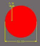
Draw a circle with the desired diameter, select it, then click "Design" => "Board Shape" => "Define from selected objects".