Continue to Site

Welcome to EDAboard.com

Welcome to our site! EDAboard.com is an international Electronics Discussion Forum focused on EDA software, circuits, schematics, books, theory, papers, asic, pld, 8051, DSP, Network, RF, Analog Design, PCB, Service Manuals... and a whole lot more! To participate you need to register. Registration is free. Click here to register now.

Buck Converter mosfet swithces problem

Status
Not open for further replies.

kah89

Junior Member level 2
Joined
Feb 9, 2015
Messages
24
Helped
0
Reputation
0
Reaction score
0
Trophy points
1
Activity points
169
Hi

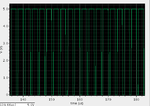
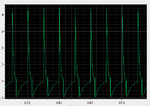
I am designing buck converter in cadence and i have some problems with the mosfet switch when I add an ideal switches and check the switching waveform it looks ok "square wave with the desired duty cycle" but when I add the mosfets the waveform changes and I don't know why. attached the schematic and the waveform images

Screenshot-13.pngScreenshot-14.png
 

Looks like feedthrough of huge gate capacitances. Curiously the PMOS transistor doesn't seem to switch on.
 
  • Like
Reactions: kah89

    kah89

    Points: 2
    Helpful Answer Positive Rating
I think you need to change the load resistance value which is shown as 400 m ohm. Increase it to atleast 10k ohm and check.
 
  • Like
Reactions: kah89

    kah89

    Points: 2
    Helpful Answer Positive Rating
I think you need to change the load resistance value which is shown as 400 m ohm. Increase it to atleast 10k ohm and check.

Nothing happened.

Looks like feedthrough of huge gate capacitances. Curiously the PMOS transistor doesn't seem to switch on.

It turns on when the gate signal is zero.
 

Looks like the PMOS transistor is slow to switch and the NMOS is not turning on.
What are the threshold voltages of the MOSFETs?
Changing the load resistor value has no effect?? It should have some effect.
 
  • Like
Reactions: kah89

    kah89

    Points: 2
    Helpful Answer Positive Rating
The frequency of the MOSFET switching is not clear in the graphs. Can you check this and simulate again with frequencies in the order of 100kHz. Don't forget to change the load resistance. 0.4 ohm resistor may not be good idea with given C and L values here.
 
  • Like
Reactions: kah89

    kah89

    Points: 2
    Helpful Answer Positive Rating
I found the problem, it was the on resistance of the two mosfets I didn't adjust it to a suitable value but now it is working. Thank you.

My last question is how to calculate the input power with cadence i tried (Iavg*V) but it is too large
 

My last question is how to calculate the input power with cadence i tried (Iavg*V) but it is too large
Iavg*V is of course right. The question is how much power is consumed by shoot-trough, simulataneous conduction of both MOSFETs. You may want to generate separate gate signals with deadtime.
 
  • Like
Reactions: kah89

    kah89

    Points: 2
    Helpful Answer Positive Rating
Thank you, It was the overlapping clock problem
 

Status
Not open for further replies.

Similar threads

Part and Inventory Search

Welcome to EDABoard.com

Sponsor

Back
Top