Continue to Site

Welcome to EDAboard.com

Welcome to our site! EDAboard.com is an international Electronics Discussion Forum focused on EDA software, circuits, schematics, books, theory, papers, asic, pld, 8051, DSP, Network, RF, Analog Design, PCB, Service Manuals... and a whole lot more! To participate you need to register. Registration is free. Click here to register now.

Altium Multisheet PCB

Status
Not open for further replies.

HWguru

Junior Member level 2
Joined
Jan 20, 2015
Messages
24
Helped
1
Reputation
2
Reaction score
1
Trophy points
3
Activity points
186
Hi ,

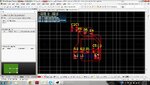
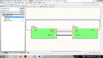
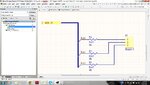
I have a Altium project with a Top level sheet . this sheet includes interconnected two sub-modules generated from separate schematic sheets e.g Sheet A and Sheet B .

But when i try to update my PCB file i.e import changes from Top sheet , i see two separate PCB rooms for sheet A and B , how can i generate one big pcb room for the Top sheet only ???

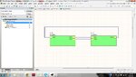
see the screen shots attached

Regards ,
 

Attachments

  • Untitled.jpg
    Untitled.jpg
    188.4 KB · Views: 112
  • Untitled1.jpg
    Untitled1.jpg
    235.8 KB · Views: 101
Last edited:

Having rooms is only useful when you're working with multi channel designs, i.e. multiple identical instances which you wish want to route once and then copy placement and routing from one channel to the others.

However, since your design is really simple (only 10 components) and you won't benefit from multi channel design features, there is no point in keeping the rooms. Simply disable rooms for these sheets.
 
  • Like
Reactions: HWguru

    HWguru

    Points: 2
    Helpful Answer Positive Rating
actually i am quite new to PCB design using altium , so please ignore my lack of knowledge . I did tried it , going into project options and disabling check boxes for "Generate room" and leaving one box checked in front of the TOP sheet, but then i see all the components are seen on top of a grid , how do i know if i start routing which layer i am working on ???
 

In the layout page there is a bottom tab,that tab contains all the layers whatever you are enabled and each layer have different color.
 

In the layout page there is a bottom tab,that tab contains all the layers whatever you are enabled and each layer have different color.

OK , i see them , so how do i define a square or rectangular area of my PCB ? with all the layers confined in that area .
 

here is what i see , without rooms enabled
 

Attachments

  • Untitled2.jpg
    Untitled2.jpg
    436.6 KB · Views: 107

U mean board shape????

then,go to this link **broken link removed** and follow the steps under this title Defining the Board Shape From Selected Objects
 
  • Like
Reactions: HWguru

    HWguru

    Points: 2
    Helpful Answer Positive Rating
You need to define your board size with the KeepOutLayer.
After select all the net from this layer and make Design-> Board Shape -> Define from selected object
and you will have something like this
PCB.jpg
Good luck
 
  • Like
Reactions: HWguru

    HWguru

    Points: 2
    Helpful Answer Positive Rating
yes..exactly...I think HWguru is new in Altium designer. So better try with square and rectangle. :thumbsup:
 
  • Like
Reactions: HWguru

    HWguru

    Points: 2
    Helpful Answer Positive Rating
The form of the board doesn't matter you just have to draw it and select all the limits : SHIFT + left clic.
I've one question ;-) Is it possible to remove the room because each time I make a PCB update I've to remove them , it is boring.
 

yes...there is an option. Go to project>>project options>>class generation and uncheck generate room option. :thumbsup:
 
  • Like
Reactions: HWguru

    HWguru

    Points: 2
    Helpful Answer Positive Rating
Thanks for the guidance , really appreciate it

I have run into more errors , the errors come up when i compile my design . its says :
[Error] TOP.SchDoc Compiler Duplicate Net Names Element[-1]: BI (Inferred)

Although after reading multiple posts and answers on it i have changed the name of the BUS input port but i still get these errors . See screen shot attached .
 

Attachments

  • Bus_error.jpg
    Bus_error.jpg
    227.9 KB · Views: 101
  • Bus_error_sheetA.jpg
    Bus_error_sheetA.jpg
    235.2 KB · Views: 95
Last edited by a moderator:

As far as I know, in Altium, you can't use a bus to carry signals from one sheet to another. The purpose of a bus is primarily to reduce the number of lines on a schematic to increase readability. In your application, it would be appropriate to use a signal harness to group the 3 lines together since I assume they're somehow related. A signal harness is a perfect choice to group logically related nets.

A port marker will snap to a harness (and automatically turn blue to indicate it's connected). You can then route the signal harness to other sheets, spit it etc.

Good luck!
 
  • Like
Reactions: HWguru

    HWguru

    Points: 2
    Helpful Answer Positive Rating
To make matters worse my Altium Designer 10 has stopped working at all , i was getting some error messages in the past like memory location violations , but i ignored them , and now it has stopped working at all . It loads up and shows my last project , but when i click on any of my files i get a message that DXP.exe has stopped working . :-(

Please any clues , as i dont want to uninstall it and go through installation procedure again .

- - - Updated - - -

Hi ArticCynda, i posted a thankyou note for you , but it was deleted by the moderator
 

Hi ArticCynda, i posted a thankyou note for you , but it was deleted by the moderator
Users who don't bother reading forum rules know why.
 

[Moved]DXP.exe of Altium stopped working

Hi ,

I was working on my PCB design project using Altium and To make matters worse my Altium Designer 10 has stopped working at all , i was getting some error messages in the past like memory location violations , but i ignored them , and now it has stopped working at all . It loads up and shows my last project , but when i click on any of my files i get a message that DXP.exe has stopped working .

My OS is windows 7 .

Please any clues , as i dont want to uninstall it and go through installation procedure again .
 

Status
Not open for further replies.

Part and Inventory Search

Welcome to EDABoard.com

Sponsor

Back
Top