Continue to Site

Welcome to EDAboard.com

Welcome to our site! EDAboard.com is an international Electronics Discussion Forum focused on EDA software, circuits, schematics, books, theory, papers, asic, pld, 8051, DSP, Network, RF, Analog Design, PCB, Service Manuals... and a whole lot more! To participate you need to register. Registration is free. Click here to register now.

Driving mosfet in buck converter

Status
Not open for further replies.

deepakchikane

Full Member level 3
Joined
Jul 17, 2012
Messages
178
Helped
2
Reputation
4
Reaction score
2
Trophy points
1,298
Location
Mumbai, Maharashtra, India, India
Activity points
2,623
buck_new.JPGDear all,
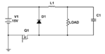
can anyone help me to drive a mosfet through a controller.

i want a better control circuit to drive the mosfet (upper)

pls find my circuit..

i cannot get idea how to drive mosfet
1)by mixing both ground..??
2)by tieing controller gnd to source of mosfet..??

any idea..??

circuit conflicts while accurate design??
 

You have messed up the circuit. Sorry but the circuit is incorrect. Just check-out the grounds!!
Why do you want to put the load at the low side?
 

You have messed up the circuit. Sorry but the circuit is incorrect. Just check-out the grounds!!
Why do you want to put the load at the low side?

Man,

this is a buck converter if you aware of it then you will realise..

m looking for solutions not the bugs
 

Man,

this is a buck converter if you aware of it then you will realise..

m looking for solutions not the bugs

With all due respect I have to say that if that is a buck converter then so is the one attached below. (see attachment)
You are already so full of your own ideas that you are interpreting suggestions as bugs!
And yes I am very well aware of buck converters but still I don't realize what you want me to! Can you still justify why you wanna use the MOSFET at the high side?
 

Attachments

  • Capture1.PNG
    Capture1.PNG
    9 KB · Views: 70
What do you mean by... "live paths", "negative paths"?
There is simply one closed loop path during the charge period. And the MOSFET can be inserted anywhere as per convenience of the ground.
 

for low voltage, low side switching is ok. For high bulk voltage such 400V dc rail, low side switching will cause a lot of emi issues.
 
What do you mean by... "live paths", "negative paths"?
There is simply one closed loop path during the charge period. And the MOSFET can be inserted anywhere as per convenience of the ground.

Theoritically concept understand..

but not working in board..

IT IS GIVING AS IT IS O/P AT 100 KHZ
 

First things first.... NEVER USE A MOSFET WITHOUT CONNECTING ITS GATE-PIN.
If not obvious, it is very likely that you will burn it off! This is due to partial charging of Gate-Source parasitic capacitor. This triggers the MOSFET into partial conduction and due to high Rds-on the MOSFET burns off.

Posting the schematic will be worth it!
 
Status
Not open for further replies.

Similar threads

Part and Inventory Search

Welcome to EDABoard.com

Sponsor

Back
Top