Continue to Site

Welcome to EDAboard.com

Welcome to our site! EDAboard.com is an international Electronics Discussion Forum focused on EDA software, circuits, schematics, books, theory, papers, asic, pld, 8051, DSP, Network, RF, Analog Design, PCB, Service Manuals... and a whole lot more! To participate you need to register. Registration is free. Click here to register now.

How to Make this type of Package in CadSoft Eagle??

Status
Not open for further replies.

xpress_embedo

Advanced Member level 4
Joined
Jul 5, 2011
Messages
1,154
Helped
161
Reputation
396
Reaction score
189
Trophy points
1,353
Location
India
Activity points
10,591
Hello!! I am using CadSoft Eagle for PCB Designing Purpose.

I need to use the GPS Module in one of my Project, the GPS Module we are using is Telit Jupiter JN3.

I want to know how can i make package shown below in Eagle.
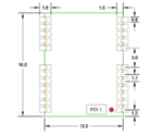
Package.PNG

I am also attaching the hardware design file for Telite GPS Module.
View attachment Telit_Jupiter_JN3_Hardware_User_Guide_r2.pdf
 

Hi,

The green lines are the package outlines of the telit device. Paint this into the dimension layer.
All the pads are shown in size and position. Draw all as smd pads. Mind the correct numbering/naming of the pads.
Place all so, that point (0/0) is in the center of the package.
Add name and value, and a sign for pad 1.
To be compatible to smd assembling machines: turn the package 90 degree cw.

Hope that helps.

Klaus
 
Getting the center-to-center distances and positions right-on can be tricky. 1) You can use the grid as a snap too to get them right, which may involve using more than just two grids; 2) You can use the "information" tool to adjust positions; and 3) You can use the command line to set the positions.

If you are a very new user and not familiar with the command line, options #1 and #2 are probably easiest. Eventually, if you do much of this, you will find the command line is easier.

John
 
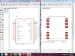
Finally I make my package.
Here is the Snapshot of the Symbol and Package Drawn.Package.png

- - - Updated - - -

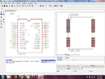
When used in Schematic and PCB Design.

Package.png
 

Hi,

looks great!.

do you want the lower horizontal line in the symbol in another layer than "symbols"?

btw: in symbol you don´t need all the nc pins. also you don´t need to place the pins in the same order as in package. But nothing wrong if you do so.

Good luck
Klaus
 
do you want the lower horizontal line in the symbol in another layer than "symbols"?

I dont understand this line.

Yes i know all pins are not necessary, i will update it soon.
Thanks for this point.

- - - Updated - - -

https://www.edaboard.com/threads/316447/
Can anyone help me on thia thread
 

Hi,

do you want the lower horizontal line in the symbol in another layer than "symbols"?
In the symbol there are all red lines but one grey line....


Klaus
 

Status
Not open for further replies.

Part and Inventory Search

Welcome to EDABoard.com

Sponsor

Back
Top