Continue to Site
Follow along with the video below to see how to install our site as a web app on your home screen.
Note: This feature may not be available in some browsers.
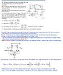
No, this is not why we connect D and G of M3 together. M3 together with M4 form a current mirror circuit.Could you explain why we connect D and G of M3 together? I think it is to make sure that M3 will be in saturation.
You don't need to worry about M6, the negative feedback will take care of it and force M6 into saturation.And could you explain how to force M6 to be in saturation?
In order to force M6 in saturation use output voltage swing specification and find Vdsat of M6 ( min Vsd for saturation ) and then take a safe value in order to keep it in saturation. I hope you are getting my words.....
That seems interesting. Could you explain more or tell me some references?You don't need to worry about M6, the negative feedback will take care of it and force M6 into saturation.
All you need is to close the negative feedback loop. Because this type of a amplifier will always work with negative feedback.
")
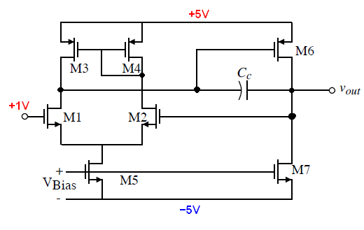
Do we need to worry about this in the firs place ? What will happen if M6 enter triode region?In the case above, the author chose Vsg6 = Vsg4 = constant. So, the saturation voltage of M6 will also be fixed and equal to Vsg6 - Vtp.
To make sure that M6 is always in saturation, we need to control output voltage swing so that Vsd6 > Vsd6(sat) = Vsg6 - Vtp.
But this seems a bit complicated. How can we control output voltage swing?
vo = VO(dc component) + Vo(ac component)
Vo(ac component) = Av(voltage gain)*Vin.
To control voltage swing, which one should we change?
@jony:
That seems interesting. Could you explain more or tell me some references?
2. The minimum value can be derived from the saturation condition of the tail mosfet M5
M5 is in saturation if Vbias - Vth5 <= VDS5
Now, VDS5 = VS2 (the common source node) and VS2 = Vin - Vov2
Therefore, Vbias - Vth5 <= Vin - Vov2 or Vin >= Vbias - Vth5 + Vov2
Could you confirm this? To satisfy the equation above, we choose bias voltages as follows.3. So select a Vin such that the above equation is satisfied. (Keeping M2 in sub-threshold not only helps in increasing gm but also helps in operating the amplifier with a lower Vin as Vov2 is lower than in saturation)
4. Now approaching the saturation condition of M2 i.e the input differential pair.
This is restricted by the upper range of ICMR ( for PMOS input pair its just the reverse)
Here we will first assume Resistor load (similar to the 2nd picture in our post) then we will move to MOS load
(a) R Load:
With R load the Vout2 = VD2 = VDD - I*RD
For saturation of M2 ..... VD2 >= VG2 - Vth2 or Vout2 >= Vin(max) - Vth2 or VDD-I*RD >= Vin(max) - Vth2
So the maximum input common mode = Vin(max) <= VDD - I*R + Vth2 (Reducing the value of R will increase the maximum input voltage but will reduce gain)
(b) PMOS Load (in your 1st picture):
VD2 = VDD - VSG4
So the maximum input common mode = Vin(max) <= VDD - VSG4 + Vth2 (VSG4 can be reduced to increase the maximum input voltage)
5. Keeping the load M4 in saturation is easy. It shares a common VSG with M3 which is diode connected. As a differential amplifier is perfectly symmetrical so VD3 and VD4 are same, as if virtually shorted.
VD3 = VG3 = VG4 = VD4 so both M3 and M4 are inherently in saturation. You just need to control the VGS value to keep M2 and M1 in saturation as discussed in point 4.
I found that will violate balance conditions in the lecture.2. Once the size ratio is fixed the current ratio is also fixed we can size the M7. M7 will have same unit W/L as M5. To change the current multiplier can be varied (as mentioned in point 1)
4. Proper balance of current:
(a) Say M5 has current I so M4 and M3 will have I/2 current
(b) If you want to burn 2I current in M6 then size of M6 will be 4 time of M4. i.e. W/L6 = Four times (W/L4) = 4 multiplier * (W/L4)
(c) M7 will be twice as big as M5 so in the last branch both the M7 & M6 are burning 2I current. So the current is balanced.
You can design in any way but you have to take two points in consideration ( for low power small sized MOS );
(1) Vsg > -Vtp
(2) Vsd > - Vdsat
Could you explain a bit more?However I think #2 is more convenient as you know ICMR thus calculate in terms of Vg1.
Well, it is strange. I will simulate it and posted the result.I am explaining for the case when MOS length is less than 1u, under this situation Vdsat is not eqaul to overdrive voltage. Although Vdsat depends on Vov and in this case you are not able to calculate Vds directly. You can verify it in CADENCE.
That means we have to specify the maximum output voltage first?Do we need to worry about this in the firs place ? What will happen if M6 enter triode region?
The output voltage will be clipped. So M6 will limit the maximum positive output voltage.
And all amplifiers has specified output voltage swing. The maximum positive or negative peak output voltage that can be obtained without wave form clipping. So Vin_max = Vout_max/Av
Av = gm1 (ro1 || ro3) * gm6 (ro6 || ro7)Find Vout and Vsd6 for this circuit
Ya, I see.2) Regarding the Vbias: Yes after the 1st step we get the current and the Vbias fixed. But the VGS2 is in our hand. We can size the M2 such that VGS2 just less than Vth, which will operate M2 in sub-threshold.
If we decrease the W/L the VGS2 will start increasing and it will cross VTH2. At this time M2 will operate in saturation. So its out choice how to size and operate M2
I think I get the point.5) By symmetry I meant equal current distribution. Yes I agree with the author that M4 is hard to keep in saturation if I had a simple CS amplifier or in a double ended differential amplifier ..... so we go for Common mode feedback (CMFB) in case of double ended output .... But in single ended its not a problem at all .... You can design one and see in Cadence ... Its is hard to explain here but the diode connected MOS, M3, actually is providing a CMFB. ....
It is really hard to prove this point .... so just test and see that VDS3 = VDS4 in open loop ..... (as I said earlier in closed loop VDS4 is not equal to VDS3 there the design approach will be slightly different)
7) This is correct... what I said I exactly the same .... If you use 2*Id5 in the second arm them W/L6 will be twice of W/L4 and W/L7 = W/L5 ..... that is what the equation in the lecture says .... but say if you need 5 time current then will it still not be in balanced condition ???? Of course it will be if you size them correctly .... for 5*Id5 the W/L6 = 10W/L4 and W/L7 = 5*W/L5 so this also gives us the same equation as in the lecture ...... thats what I meant
Could you explain why VDS4 is not equal to VDS3 in closed loop?
You as a IC designer need to design a circuit that give us as much output voltage swingThank you, Jony.
That means we have to specify the maximum output voltage first?
P.S. I think in this case, we consider the op-amp ideal. And so, Acm = 0.
Vout = (1- Vout)/2 * Av
or Vout( 1 + Av/2) = Av/2
Vout = Av / (2 + Av)
If Av is very large, Vout = 1V.
Vsd6 = Vs - Vd = 5 - 1 = 4V.