Continue to Site
Follow along with the video below to see how to install our site as a web app on your home screen.
Note: This feature may not be available in some browsers.
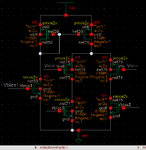
It is used for LDO with Vout = 2V.Well I think we may need to know more about the application.
The output voltage is feedbacked to V+ and is compared with reference voltage V - = Vref = 1.5V.. The biasing voltages are obviously used to turn on the gates depending on what you are trying to compare and when the signal should be triggered or not.
Vbias1 should be the level to activate the total amplifier and drive the PMOS low to turn them on.
Vbias3 passes either V+ or V- depending on what you are comparing. For all this work, this seems like an easy job for an op-amp to do and looks similar to the internal structure of an op-amp.
... how to to choose bias voltages, Vbias1, Vbias3 here? What is the calculation needed to do?


")
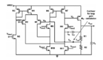
Could you explain more? And what is O/P node?You circuit is totally wrong .... where is the O/P node of your the amp that you are designing........
This is the part that I don't quite understand.(c) The rest of the circuit is a folded cascode error amplifier (error amplifier is just a trans-conductance amplifier)
It would be great if you could explain about O/P node.(d) Vg is the O/P node of the error amplifier
May I know the reason? Why they should be in saturation?2) M10 & M11 must be in saturation. The gain of the error amplifier alone is approx = gm1 * (ro7 || gm*r09*ro11)
No, they should operate in saturation mode in order to maintain good current regulation.1. Do M10 and M11 need to be biased so that they act as resistors?
It's the Cc capacitor. Its purpose is to reduce the unity gain bandwidth (UGB) of the amplifier, thereby increasing its phase margin (PM). Also, see SIDDHARTHA HAZRA's answer.2. The paper says that the regulator is based on a folded cascode differential input stage with a current buffer compensation. Could you point out where is the current buffer compensation? What is its purpose?
Because this is the standard method to bias CMOS circuits. An extensively constant current - often created via a band gap reference voltage - supplies current mirrors, which create the bias voltages. Currents can be easily divided or multiplied via the mirrors' W/L ratios.3. Could you explain why did you choose the bias circuit like that?
See above!4. What is the role of capacitor Cc in the picture?
Right!Could you confirm if it is correct or not?
Opps. I detected a mistake. M9 should be diode connected.
Could you explain more? And what is O/P node?
The rest of the circuit is a folded cascode error amplifier (error amplifier is just a trans-conductance amplifier)
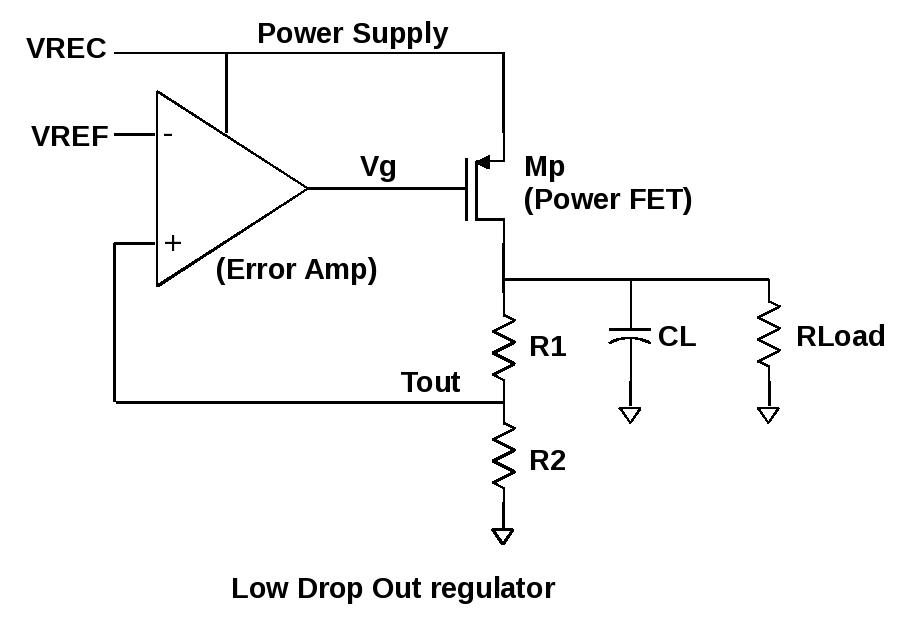
I usually see M10 and M11 are replaced by resistors. What is wrong with that?
1. M5: it is biased to operate as a current source.
2. M3 and M4: they together form "current mirror".
3. M1 and M2: differential amplifier.
4. M6 and M7: current mirror
5. M8 and M9: really can't get it, what is its function?
6. M10 and M11: they seems to be current sources (as you said)
I see M1 and M2 form differential but could you tell me where is the folded cascode?
The output of error amplifier is a current, right?
Vg will be equal to the current multiplied with the input impedance of PMOS output stage Mp.
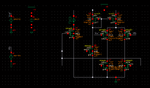
I chose Vbias1, Vbias2, and Vbias3 all above the threshold voltage of NMOS transistors a little and therefore, M5, M8, M9, M10, and M11 all are in saturation. However, the problem here is that all the rest transistors are NOT in saturation.
...
All these transistors should be in saturation but I can't figure out how to do that.
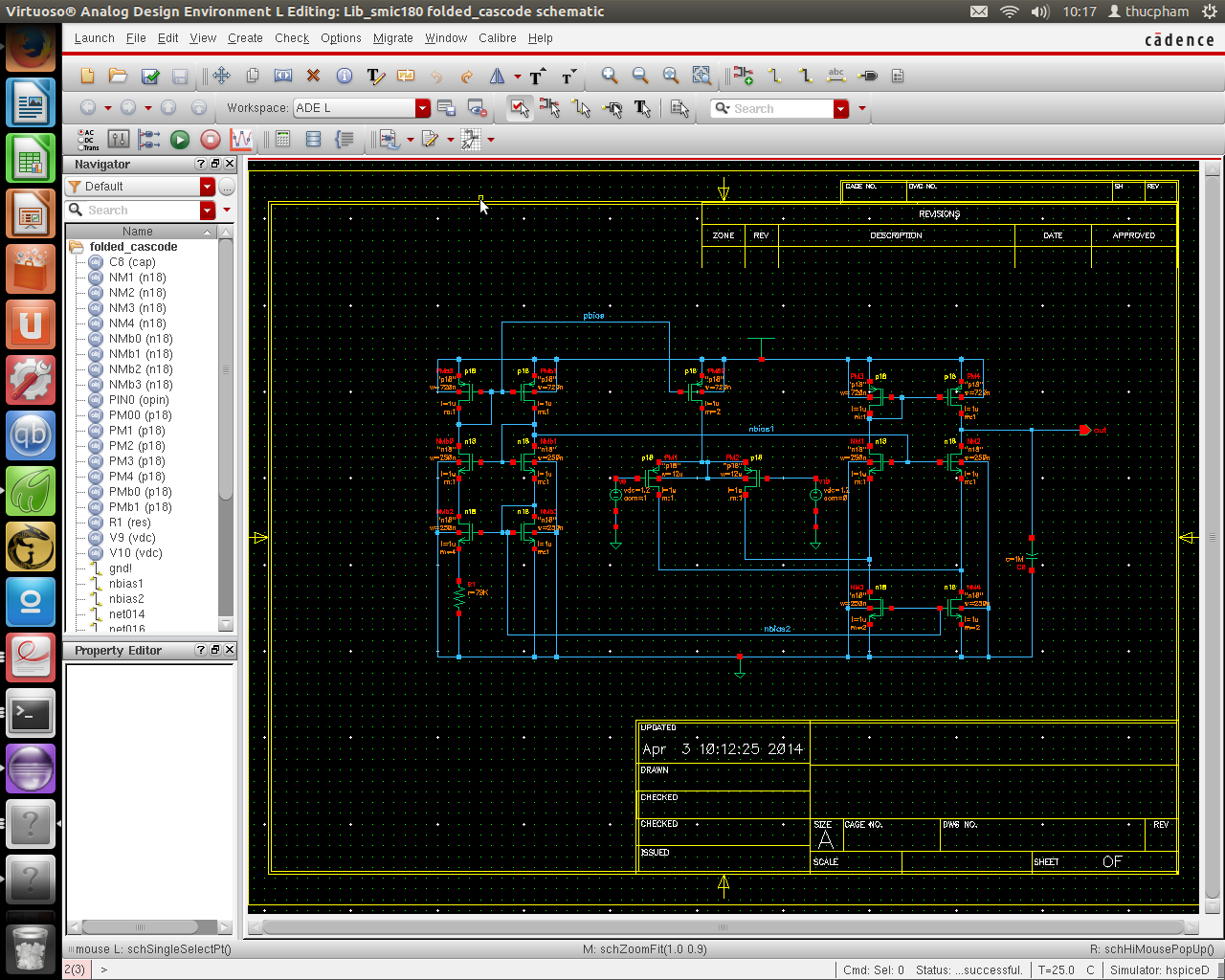
Yes. I will post it later. At present, I use ideal dc source to bias. I need to replace it by a biasing circuit.If you need further help, show the circuit diagram with voltage values at all the nodes.