neazoi
Advanced Member level 6
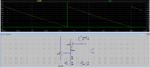
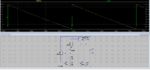
I refer to the circuit in post #17.
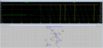
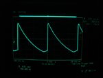
I have used 2k2 for R2 and 47R for R6. These were the only changes. I do not know why is it so non-linear, any ideas?
For the cap I used 100nF. 30 Hz and lower is perfect for my application but I would like ot fo be linear.
Now about the hot transistor,
Ok I left the R6 connected durring tests on 50R and also 1M. This was not right and that was why the transtistor was probably getting hot. Maybe I should replace it with 1M, to match my scope's 1M input and to limit the current to the transtistor? 50 ohm is not really needed for this application. I do not like to have the internal load of the oscilloscope dissipating all the power of the amplifier so I think I am going to include this R6. But then R6 in parallel to the internal resistance of the scope will do 500K. Is that a problem?
")