Continue to Site

Welcome to EDAboard.com

Welcome to our site! EDAboard.com is an international Electronics Discussion Forum focused on EDA software, circuits, schematics, books, theory, papers, asic, pld, 8051, DSP, Network, RF, Analog Design, PCB, Service Manuals... and a whole lot more! To participate you need to register. Registration is free. Click here to register now.

How to add custom library or own library in Altium ??

Status
Not open for further replies.
Hi hemnath,
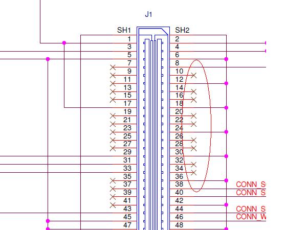
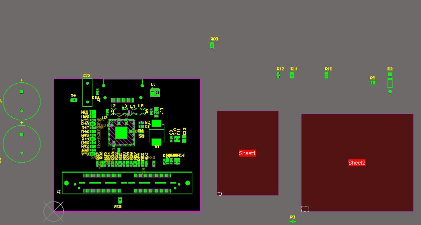
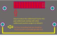
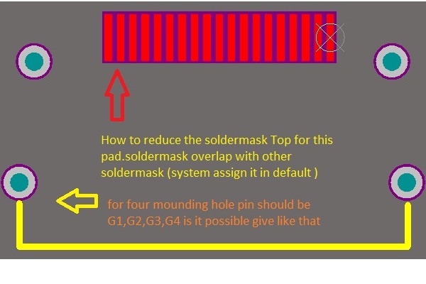
still i am learnt footprint creation.i posted one HDMI connector footprint.in this i have doubt in that please clarify it

- - - Updated - - -


Yes you can change the soldermask in the rules section.

Design-> Rules->Mask-> soldermask expansion. There you can edit the values.

For mounting holes, double click the pad and edit the designator as your wish :)

Best wishes :)
 

you can edit the soldermask in PCB. Not in the project library.

I am not sure whether you have find the solution or not. Sorry for late reply. I was quite busy with my project works.

Best wishes :)
 

how to make pin as unconnected pin ??

- - - Updated - - -

how to edit symbol in Altium ??
 

What do you mean? i don't get you.

When the pin is not connected to any other component, it is left blank and the net is not assigned to that pin.

You cannot edit symbol in Altium schematic. You can only edit in the library.

Best wishes :)
 

can you this one ?? i could not annotate the design.please reply
 

Attachments

  • check.rar
    47 KB · Views: 82

I think, you have opened the schematic as a free document, so you will face the troubles.
Try to add your schematic to a project, then annotate the design.

Best wishes :)
 
HI,
i am trying to create footprint (i have not get any easy method to create PCB footprint ) do you have any document regarding this.while creating footprint i could not reduce the soldermask and paste mask pad size.is there any option ??
 

While creating a footprint in the library, double click the pad which you want to change the soldermask expansion.

It will pop up a window "PAD". You can see options like "Paste Mask Expansion" and "Solder Mask Expansions". In that, click "specify expansion value" and change the value as required.

Best wishes :)

- - - Updated - - -

While creating a footprint in the library, double click the pad which you want to change the soldermask expansion.

It will pop up a window "PAD". You can see options like "Paste Mask Expansion" and "Solder Mask Expansions". In that, click "specify expansion value" and change the value as required.

Best wishes :)
 
hi how to make mechanical pin ?? is there any other way to make footprint easily.i am taking more then 30 min *(manual creation not IPC standard)
 

What do you mean by mechanical pin???
Everything comes faster by practice ...

Best wishes :)
 

hi Hemanth,
thanks for your reply. while copying pad pad is away from cursor location.how to resolve it

- - - Updated - - -

3709267800_1378811925.jpg


- - - Updated - - -

i could not see the footprint in my library here i attached QTH-060-04-L-D-A symbol and footprint please check it

- - - Updated - - -

please reply for this post
 

Attachments

  • check2.rar
    15.7 KB · Views: 58

Hi hemnath,
After long time, i am come to learn altium,i was little bit busy with my job.Right now i am doing placement for one board.i need to change the Height of the reference designator for all components (i could not change one by one )please let me know how to change it
i need some clarification in following this
1.After importing DXF is i need to make manually outline for board outline ??
2.how to highlight the net or power pin ?? for example Ground and Power
3.is it possible to make placement view in layout (in allegro or pads we can make placement view - assembly line,silkscreen line top,ref des, board outline)

- - - Updated - - -

how to hide the all the reference designator in board
 

Hi kapil,
Hope you are doing good.

To change the height of designator: you can see an option "PCB" at the bottom right corner. Click it and open "PCB filter". It will pop up and type "IsDesignator" in find items matching these criteria. And click ENTER. It will select all the designators in the schematic. Now press F11. It will Open PCB inspector. In that, edit the designator Height and width in one shot.
1.To my knowledge, Yes you have manually outline for board outline.
2.when the place the cursor on any net, it will automatically gets highlighted.
3.Do you mean by filtering the layers??
Top overlay and bottom overlay are used for Designators. By hiding the selected layer, you can hide the designators.

Best wishes :)
 

Hi hemnath,
Thanks for your reply. is i need to keep the sheet1 and sheet2 inside the board as shown in Picture below
 

how to move the component in bottom (i need short cut )??
i completed the placement but i need to align the component 15 mil (component to component )distance for keep fanout is it possible ??
 

it is not necessary to keep the sheets. You can delete it. View Altium videos, then know why the sheets are used.

To move the component in bottom, select the component and press L .
Use rules option for component to component distance. Attached is shortcut keys for your reference.
 

Attachments

  • Altium_GU0104_Shortcut Keys.pdf
    190.6 KB · Views: 69

Hi hemanth,
Thanks for your reply. i think you might be busy.sorry for disturb.i learnt little bit altium still i could not learn clearance and constraint settings could you please checkt the board file and schematic and correct the error and let me know the details of error and how to solve it

- - - Updated - - -

please update corrected PCB and schematic to me if you get to solve this problem.please guide me how to set the constraint setting for spacing ,electrical,differential pair
 

Attachments

  • check1.rar
    303.4 KB · Views: 62

Status
Not open for further replies.

Part and Inventory Search

Welcome to EDABoard.com

Sponsor

Back
Top