Continue to Site

Welcome to EDAboard.com

Welcome to our site! EDAboard.com is an international Electronics Discussion Forum focused on EDA software, circuits, schematics, books, theory, papers, asic, pld, 8051, DSP, Network, RF, Analog Design, PCB, Service Manuals... and a whole lot more! To participate you need to register. Registration is free. Click here to register now.

Help need for drawing IIP3 and P1dB using AWR MICROWAVE OFFICE.

Status
Not open for further replies.

btv_murthy

Full Member level 3
Joined
Nov 29, 2011
Messages
159
Helped
9
Reputation
18
Reaction score
9
Trophy points
1,298
Location
BANGALORE
Activity points
2,719
Dear Sir,
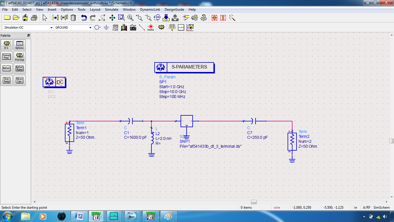
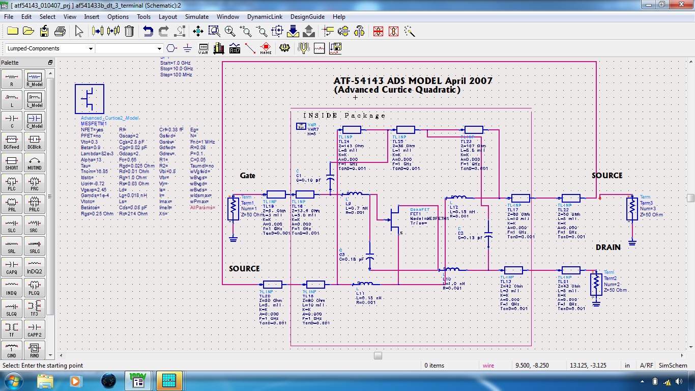
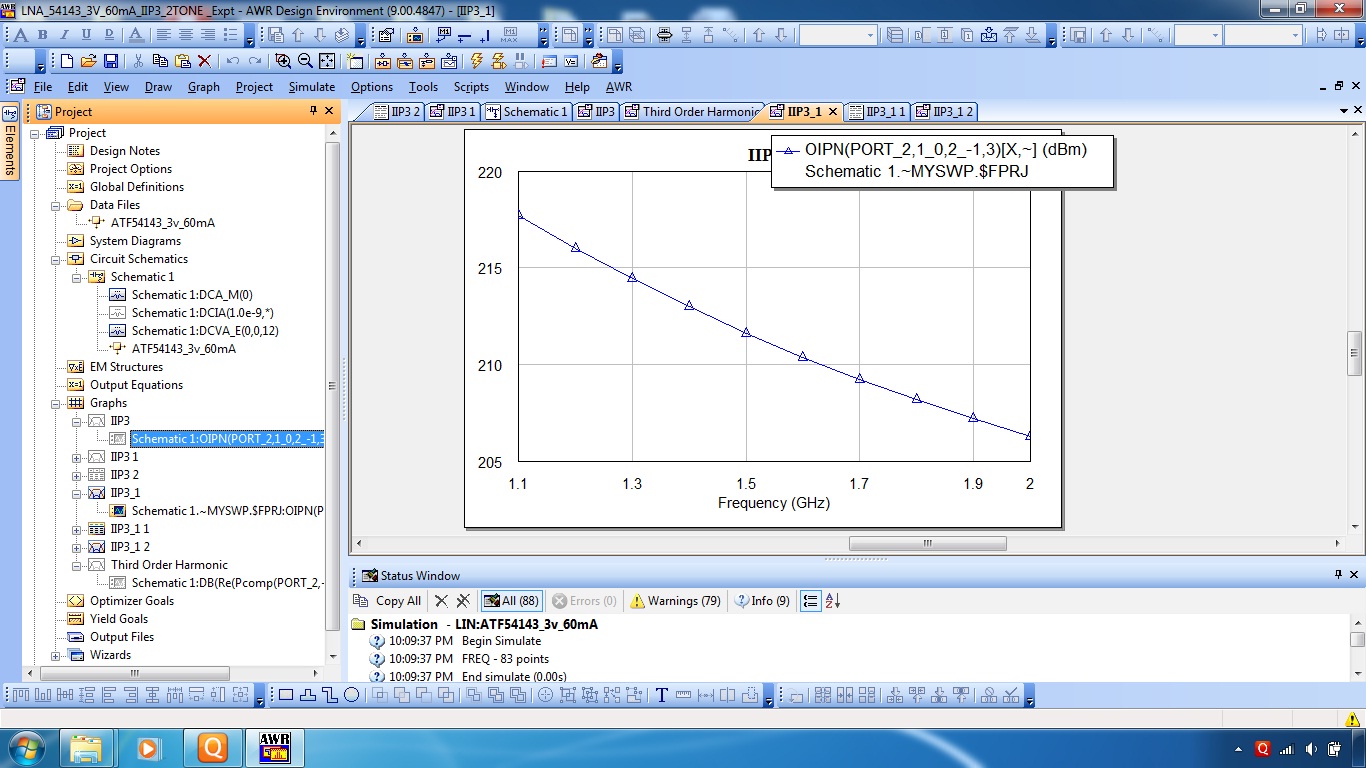
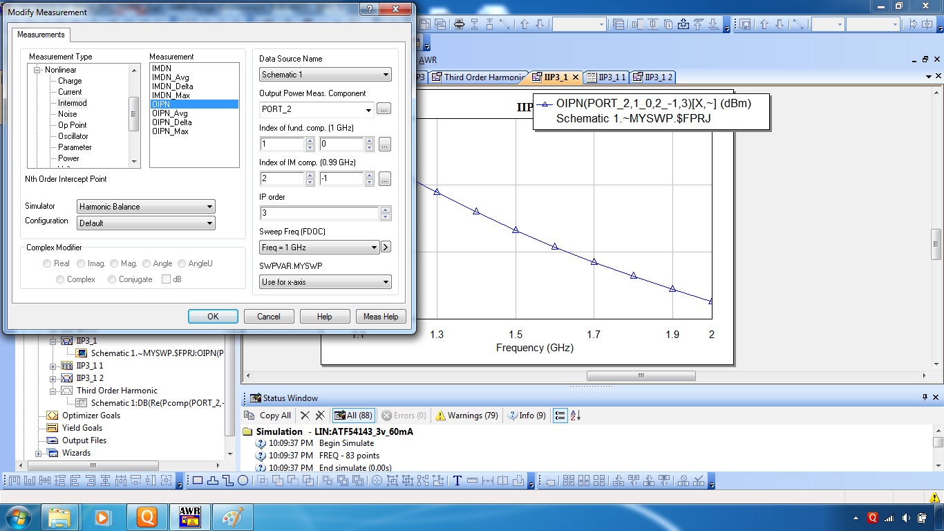
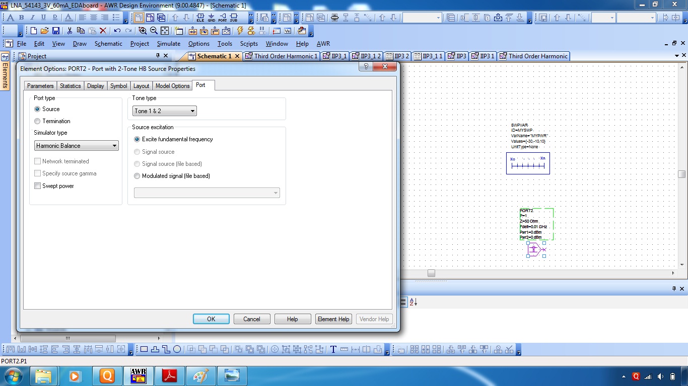
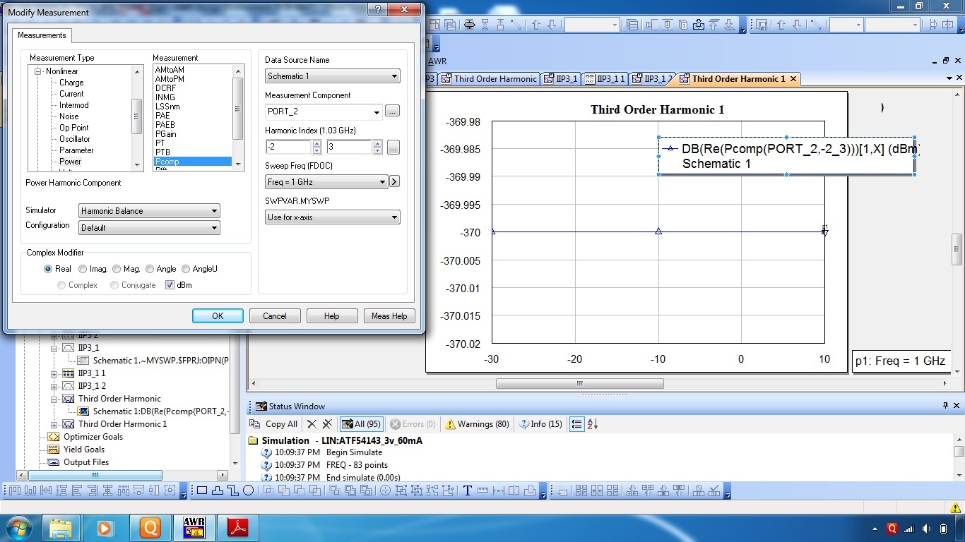
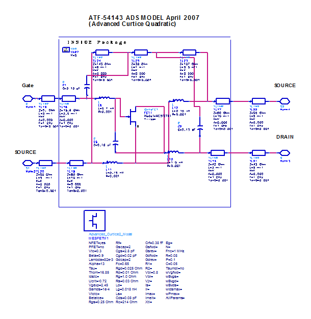
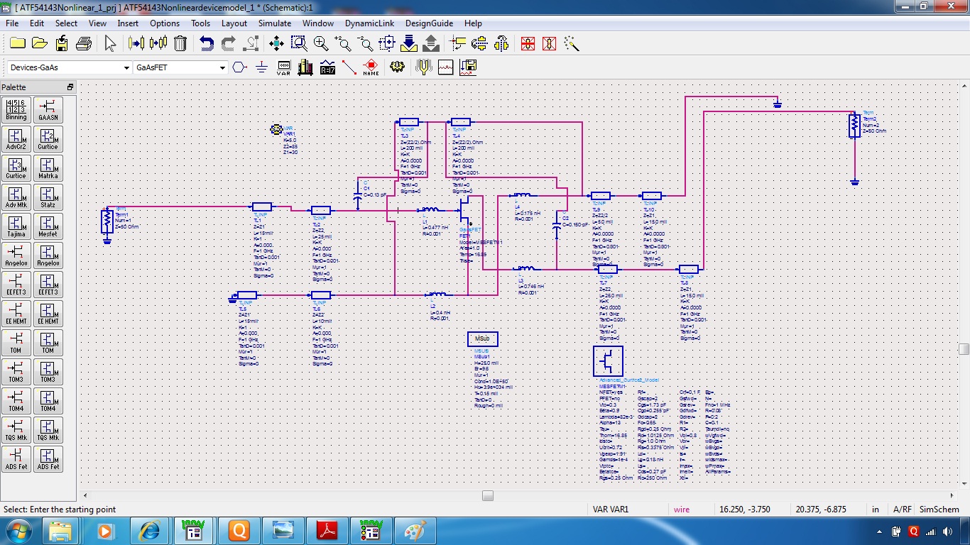
I have designed low noise amplifier at 1.3 GHz , got gain as 16dB and NF as 0.7dB using AWR MICROWAVE OFFICE. Now I want to draw and measure IIP3 ,IM3 and 1dB compression point using AWR MICROWAVE OFFICE. Can you anybody help me to draw and measure IIP3, IM3, P1dB using AWR microwave office.
 
Last edited:

Dear Sir,
I am attaching the simulated results to corresponding posting #1, have got the ( for graph Frequency vs IIP3)IIP3 as 214dBm and for graph of Pin(dBm) vs Pout(dBm) got -270dBm. Can you anybody help me, what mistake I am making and what changes I have to make for getting proper results.


Looks like you are using the s-parameter model for the ATF-54143 (@3V 60mA) for the active device. This will only give you the capability of performing swept frequency linear measurements, i.e. S21, S11, noise or stability type measurements etc. It does not facilitate any power dependant measurements. The model cannot create harmonics to measure intercept point or compute compression measurements.

The 3rd order output graph is basically at zero as far as the simulator can measure, i.e. no 3rd order output. There is no simulator that can do this with a s-parameter model. You need a non-linear/Spice like model to do this simulation.
 
ADS has X-parameters can do so, but I haven't tried yet.
 

RealAEL Sir,
As you said without nonlinear device/spice model, we can't obtain IIP3,OIP3, P1dB, thirdorder harmonic. For my low noise amplifier at 1.3GHz( transistor is AVAGO ATF 54143) which nonlinear device is suitable. which nonlinear model/spice I have to choose. Shall I choose NE71300. I have shown in the image nonlinear device, shall I choose shown in the image nonlinear device or choose someother nonlinear device. Can you help me.

Every transistor has its own model, you can not use another model for that..

Your ATF 54143 is obsolete but you can find models,s-parameters etc in this page.


The design kit has been developed for ADS.You should extract the model from this sub-circuit.
 

I would never use any device model that was not for the actual device itself. Using a model for a different device from a different manufacturer make no sense at all.

Avago provides a **broken link removed** based on the **broken link removed** for ADS 2009. That is where I would start.
 
Every transistor has its own model, you can not use another model for that..

Your ATF 54143 is obsolete but you can find models,s-parameters etc in this page.


The design kit has been developed for ADS.You should extract the model from this sub-circuit.


Dear BigBoss and RealAEL sir,
As you told ATF54143(AVAGO)transistor is obsolete. Has it limited application in market? is not it much usefull. I have designed my LNA at 1.3GHz using MWO with ATF54143. Is it difficult to fabricate? in what way it is obsolete?. Can you make it clear. One more doubt, In datasheet of AVAGO 54143, they have created ATF 54143 curtice ADS model and also used transistor as GaAS FET FET1 Mode1= MESFETM1 nonlinear device model.But I am using AWR MWO , how I can create nonlinear model without using GaAs FET FET1 Mode1= MESFETM1 nonlinear device model that nonlinear transistor model is not availble in the AWR MWO and TLINP with different parameters. What I have to do, I am in confusion, which GaAs FET FET1 I have to choose. Some GaAS curtice nonlinear device model are availble in AWR MWO . Shall I use and create nonlinear device model of those, if I use those,will it work?. Can you help me.
 

This device is NOT obsolete. Over the years the device has changed and some early versions have been replaced by later versions as the manufacturing processes evolve and develop. The obsolescence note on the Avago web page is simply stating that the device has now changed to a lead free technology so the old part number ATF-54143-TR2 has been replaced by ATF-54143-TR2G. The basic device is still available. As the web page lists it has "Lifecycle Status: Active" and there is a "Buy Now" button on the page.

With regard to the model, if Avago spent the time to build and validate a model for a particular simulation platform I would certainly be more inclined to trust the use of that model using the same platform. Transposing this model data to a different platform cannot guarantee appropriate performance.
 
Dear BigBoss and RealAEL sir,
As you told ATF54143(AVAGO)transistor is obsolete. Has it limited application in market? is not it much usefull. I have designed my LNA at 1.3GHz using MWO with ATF54143. Is it difficult to fabricate? in what way it is obsolete?. Can you make it clear. One more doubt, In datasheet of AVAGO 54143, they have created ATF 54143 curtice ADS model and also used transistor as GaAS FET FET1 Mode1= MESFETM1 nonlinear device model.But I am using AWR MWO , how I can create nonlinear model without using GaAs FET FET1 Mode1= MESFETM1 nonlinear device model that nonlinear transistor model is not availble in the AWR MWO and TLINP with different parameters. What I have to do, I am in confusion, which GaAs FET FET1 I have to choose. Some GaAS curtice nonlinear device model are availble in AWR MWO . Shall I use and create nonlinear device model of those, if I use those,will it work?. Can you help me.

7191292500_1368527839.png
 
Last edited:
RealAEL Sir,
O.K. now we can say that ATF 54143 is not obsolete. As you said about the nonlinear model creation of the ATF 54143 avago , it is not possible in the AWR MWO .But I am familiar with AWR MWO and have designed my lna using AWR MWO. Now I must have to switch over to ADS platform to create same LNA. One more quesition is, is it readymade Agilent ATF 54143 nonlinear device model availble? . If it is not availble, I must have to create ATF 54143 nonlinear device model as shown in the datasheet ,then I have to go for simuation of P1dB ,IIP3, OIP3.

2) My second doubt is, using linear device ATF 54143 designed lna and got gain, NF and input and output return lossess. For non linear simulation ( i.e. measuring iip3,oip3,p1dB)same circuit need ( what ever I used for obtaining gain , NF and input and output return lossess)to use or I have to design different circuit for nonlinear simulation using nonlinear device model. Can you make it clear.
3)Third doubt is , in ADS2009, we cann't save any file to any other directories (like E drive, Ddrive or F drive) other than C:\USER\DEFAULT. In ADS 2009 , I tried to save any file other than default directory ( i.e. C:\USER\DEFAULT), it is not allowed. Can you guide me, how to save any file other than difault directory( i.e. to E drive, F drive,).
 

1. Avago have done this for you. Download the ADS Model from their website into ADS 2009 and you will have exactly what BigBoss showed you in his last post.
2. Used the model provided by Avago and build that, with the custom symbol, into your LNA design.

ATF54143.png

Then use the resulting LNA design in each of a set of schematics required to perform the measurements you need. Probably 3 schematics, one for s-parameter & noise etc, one for DC and the third for harmonic balance to do the P1dB, IP3 etc. Look at the built-in example project under RFIC/amplifier_prj for example. Not exactly what you re doing as the design is an IC but this project includes a schematic design called PA.dsn. This is then used in three simulation 'test benches' where one does HB simulation, one does Transient simulation and one does ACPR using Envelope simulation. So you only need to create the LNA schematic once. You can use the same non-linear model to do all simulations.
3. ADS schematic designs, dsn files, should only be saved into the working project but that project can be anywhere that you can write to. It does not have to be in the default starting directory. When you create the new project simply browse to the required location on whatever drive you would like to use on the file system. The only restriction is that the path to the project, the project name and the design name cannot contain spaces.
 
RealAEL Sir,
I am sorry that I have created ATF 54143 nonlinear device model as shown in the datasheet of AVAGO ATF54143. But I am getting the so many errors , I don't know how to solve it. Can you help me remove those errors. I am attaching both nonlinear device model and error window.


[/url


[url=https://obrazki.elektroda.pl/9535701700_1368603218.jpg]
 

The K values should be "K" in TL1 and TL5 that is defined in Var block.
Change K values in these two...
And please check your circuit before requesting help here...
 
Personally I would never have attempted to create this model schematic myself if other sources were available. The model available from the Avago web site, although it is not exactly the same as the printed datasheet model, it is extremely similar and already done. The problem with working from datasheets is that errors can occur. In your case, as BigBoss pointed out there are differences in the K values you entered, although I say with your TL8 and TL10. Also it is not totally clear in your image but it looks like TL3 and TL4 have length values of 200 mil and not 20.0 mil and C2 should be 0.159 pF and not 0.150 pF but that last one in a minor difference that is probablynot too important. Perhaps more critical though is the printed value for Crf in the datasheet that you have entered as shown. It is included in the datasheet as 0.1 F with Rc of 250 Ohm. That is an impossible value for this type of device. More likely 0.1 fF would be more realistic. The pre-built model shows it as 0.38 fF with Rc as 214 Ohm. Also there is an MSUB in the schematic but it is not needed. All the transmission line are TLINPs that do not need an MSUB. That one can be deleted but a new one would need to be added once you build your LNA circuitry as necessary. You should be more thorough in your checking and look at this data more critically.

The most important issue though is the schematic you are using here. Although we cannot see everything that you did an s-parameter simulation should not be the first simulation that you complete for this scerario. Whenever you use non-linear models like this they must be appropriately biased. It is not like s-parameter data files that are measured at a particular bias configuration so that voltage sources do not need to be included in the design. For simulating this device voltages sources and any associated circuitry need to be included in the schematic even for s-parameter simulations. So just putting Terms on the Gate and Drain connections and grounding the Source pins will not generate realistic s-parameter data. To that end the first simulation that I would attempt would be a DC simulation to verify the the device is indeed operating at the required Vds & Ids bias. Once that is done then s-parameter and harmonic balance simulations could be started.
 
RealAEL Sir,
As you said, I downloaded the ATF 54143 ADS nonlinear device model from the Avago website. File is in the .ZAP format that file is pasted on the desk top and shown the path for the data item , it is showing the follower. Please help me to remove the showing error ,because I am beginner to ADS 2009. Meanwhile I created nonlinear ADS model device model as shown in the datasheet of ATF 54143, it is not working upto the mark. I am attaching two related images.


A .ZAP file is not a model data file. It is an archive of an entire project. Use the menu command File > Unarchive Project... in the ADS main window to extract and then open the project. Once you do that you will find a file ATF54143_dt.dsn that is the model schematic to use in you LNA. Don't forget though that you MUST include DC sources to bias the device to be able to perform any s-parameter simulation.
 

A .ZAP file is not a model data file. It is an archive of an entire project. Use the menu command File > Unarchive Project... in the ADS main window to extract and then open the project. Once you do that you will find a file ATF54143_dt.dsn that is the model schematic to use in you LNA. Don't forget though that you MUST include DC sources to bias the device to be able to perform any s-parameter simulation.

RealAEL Sir,
As you said using archival extracted .ZAP file. I used the ADS nonlinear device model and connected the same circuit of the linear device model(whatever circuit it is connected to the linear device). But the results are entirely different from the linear and nonlinear device model at Vds = 3V and Id= 60 mA. What is my doubt is do I need to have different circuit to connect for the nonlinear device ADS model to measure the IIP3, OIP3 and p1 dB compression point or Do I have to use the same circuit and biasing for the nonlinear device model , whatever I used for the linear device model. Do I need to use the linear device model for measuring gain , NF and Stability? Do I need to use nonlinear device model for measuring the IIP3,OIP3, P1 dB compression point or else do I need use single nonlinear model for the both measuring Gain, NF, Stability, IIP3,OIP3, P1 dB compression point.One more thing is do I need to use the linear device for only measuring for gain, noise figure and stability.
 

You definitely should be using exactly the same matching networks for both linear and nonlinear simulation cases. Bias sources are needed for the nonlinear simulation but not required for the linear simulation. However, if there is any chance that the bias networks may be effecting the matching in any way then this element of the circuit must be included in both simulations. Try doing an s-parameter simulation of just the input matching network and just the output matching network, with and withoiut the bias circuitry, and check the reflection coefficiet that the transistor would see and verify if they are the same. If there is a difference then the design is incorrect. If they are the same all is good.

More important with the bias circuitry connected to the nonlinear device are you getting Ids=60mA for Vds=3v when performing DC simulation. If you do not then comparison with that s-parameter data simulation will certainly give different results.
 
RealAEL Sir,
As you told that I have checked both linear with bias and input and output matching nonlinear with same input and output matching and biasing , results are entirely different. Also checked the with bias and without biasing nonlinear ADS model connected , for them also results are different. Where I am making mistake, biasing is set Vds=3.02v and Id=63.7mA, I couldn't find it. I am attaching the images.


Status
Not open for further replies.

Part and Inventory Search

Welcome to EDABoard.com

Sponsor

Back
Top