Continue to Site

Welcome to EDAboard.com

Welcome to our site! EDAboard.com is an international Electronics Discussion Forum focused on EDA software, circuits, schematics, books, theory, papers, asic, pld, 8051, DSP, Network, RF, Analog Design, PCB, Service Manuals... and a whole lot more! To participate you need to register. Registration is free. Click here to register now.

Continous Sigma Delta ADC- Choosing the proper DAC

Status
Not open for further replies.

mretsh91

Junior Member level 3
Joined
Jan 26, 2013
Messages
28
Helped
1
Reputation
2
Reaction score
1
Trophy points
1,283
Activity points
1,509
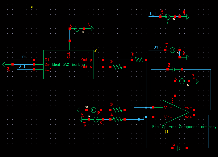
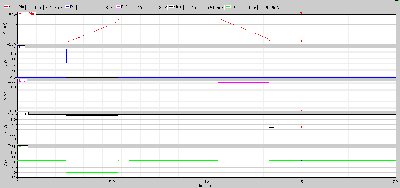
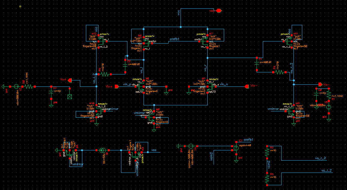
I am currently working on a fifth order continuous time sigma delta ADC, the sampling frequency used is 384 MHZ .... I have a main problem with the normal DAC using MOS-switches as it has a large delay.... what DAC architecture should I use to work fine with this sampling frequency ?????
 

What technology are you working with? I would think at 384MHz, there shouldn't be a problem. Are you sure you are compensating for excess loop delay?

JGK
 

First of all, I'd like to thank u for your concern.
Concerning the technology, I am working with 0.1um with 1.2 volt.
Concerning the excess loop delay, I am using a switch after the DAC to integrate only over the second half of the period, and of course the integration value is doubled after this.

Actually, I have implemented the DAC using ideal switches afterwards I implemented this DAC using MOS switches, the SNR was degraded by 30dB !!
So, I am sure that there exist a fundamental problem in this DAC.

The question is what DAC shall be the fastest ?????
 

Hello,

If your sampling at 384MHz in a 100nm technology, I really don't see why you would have a problem. At that rate with a current steering DAC you should be fine. Just wondering, if your loosing 30dB, what is your target SNDR? are you loosing like 80dB to 50dB? or something alot higher? If you provide an NTF before and after with DAC put it I could help more.

If I was you I would just use the fully differential current steering DAC, which switching on both sides for reduced power. If you don't care about power, then just switch one side. At your clock rate, it will definitely work.

JGK
 
Actully my SNDR target is 80 dB.
Concerning the current steering DAC, I am implementing the circuit shown and also I am including the DAC connected to the first integrator in my system.
first of all I am working with 1.5 bit DAC,so is this circuit ok ???

if so,, I have two problems in my design:

1-The mirror can't derive the current that I need as the 1.2 supply is very limiting, so how to increase this current to something like 750uA ???
2-The current mismatch between the nmos and pmos mirrors is large, and it will detriorate the performance of the system. How to get rid of this mismatch ???

thanks in advance

Screenshot at 2013-04-07 16:24:46.pngScreenshot at 2013-04-07 16:31:37.png
 

Hello Mretsh,

Well, if you are using a 1.5bit quantization then your DAC needs two cells!

Second, just wondering, but why are you using a return to zero (RZ) DAC? Why wouldn't you use non-return to zero (NRZ) since it will have better rejection to CLK jitter? I completely understand you can use a RZ DAC when your worrying about ISI, but I don't think you would have an issue since your at a lower CLK rate.

As for your DAC feedback... Why do you have those resistors there.. If you are using a current steering DAC then you don't have resistors, therefore, you just push your current into your summing node. If your using a resistor DAC, then you need those resistors then switches and reference voltages. I would not use a resistor DAC since then you need to provide these reference voltages which is a pain.

Also, you shouldn't have to worry about a 750uA current. You can totally make a current mirror with that much.

Lastly, you are correct the NMOS, PMOS mismatch will be seen there, because your not cascoding your current mirrors to greatly reduce this mismatch. But this mismatch will only produce an offset within the loopfilter and will be regulated out by the opamps CMfeedback. Since both cells, (since you are going to have 1.5bit) have the same problem this mismatch will not effect your CTDSM. BUT when you have real mismatch in both cell, like running a Monte Carlo mismatch simulation, this will effect your CTDSM, and therefore, you will need to correct for it in the analog or digital domain. At this clock rate, a DEM/DWA can be used in the feedback path, but this is limited to the OSR of the ADC. If your OSR is low, then DEM/DWA will not work very well.

Hope this helps,
JGK
 
thanks alot jgk2004 ... I appreciate your concern again ..your comments were very helpful to me.
 

Excuse me jgk2004 , i am working on that same project and i had some questions . We are facing some problems implementing the above DAC. So , are u sure that the MISMATCH between the PMOS & NMOS current mirrors won't affect the system ? ,, we are facing a serious problems and we think that maybe this mismatch offset is the reason.

In otherwords, we read in some papers about mismatch removal techniques like Calibration for ex. . Are these techniques necessary or the DAC is as simple as the above circuit??
By the way , we are working with 65nm technology..

Thanks in advance.
 

I don't see why it would be the problem. Its just a common mode problem. unless your amplifier can't regulate it out... Is your amplifier ideal? or real. if it is real put in an ideal verilogA one to see if that removes the loss in performance.
Next, try replacing the the NMOS and PMOS with ideal current sources with the EXACT same current. Then make them both equal. Of course this means you still have to have the same switches in place.

Also, is your NMOS PMOS operating in saturation? Make sure they are.

When you read calibration techniques for mismatch, they are talking about mismatch from one cell to another. since you are not doing monte carlo simulations, you dont have mismatch...

Also, when you mean you are having problems, what is happening, are you having lots of harmonics or an increased noise floor or both?

If you show me FFTs before with ideal DAC and after with designed DAC it will easier to see what the problem is

JGK
 
Thanks for your Concern .

We didn't design the Real Op Amp yet , we are now working with a behavioural model for the fully differential op-amp built out of 2 vcvs . I believe it doesn't have the mechanism of CMFB , so , maybe that's the problem as the input common mode to the Op-amp isn't constant while the DAC is connected.

So , we'll take a few days to build the Real Op-Amp and get back to u if the problem still exists.

Thanks for your help ..

Just out of curiosity, are you also using RZ DAC.? Do you see any second harmonic in the spectrum?
 

Just out of curiosity, are you also using RZ DAC.? Do you see any second harmonic in the spectrum?

We are using RZ DAC to compensate the loop delay simply
 

If you use a RZ DAC to compensate for loop delay, then you don't have any ELD compensation, i.e. having a dedicated ELD feedback around the quantizer. Also, I hope you are keeping i mind that by using a RZ DAC for compensation, you can only compensate for loop delay if its less then 25%.....
JGK
 
Yes, i don't have a dedicated ELD feedback around the quantizer , BUT unfortunately i didn't know about that 25% condition, i just thought that i would totally neglect the output of the DAC for the first half cycle ( open circuit during the first half cycle , therefore , it isn't connected to the integrator , and compensating that by multiplying the output of the DAC by 2 in the second half cycle)..

I haven't read that in a paper or text book , i just thought about it and implemented it in the matlab behavioral model.

Please tell me if i am wrong . Also , how can i test or estimate the loop delay ?
 

Providing DAC feedback during the second half clock cycle defeats the purpose of using RZ DAC. The feedback should be during first half clock cycle, and return to zero or return to open in the next half cycle. This way half the clock cycle delay can be tolerated.
 

What you are describing is exactly what RZ feedback is, but you simply can not just forget about the first 50%. Normally, lets say a really slow CLKed design, you would have your RZ feedback pulse in the first 50% since the Quantizer would be FAST (or small delay)... then zero for the second half. it would still have to be 2X in height compared to the NRZ pulse so it will provide the same amount of charge per-cycle..
but you are delaying it by 50%. This will results in all of your integrator swings increasing alot and if clipping occurs, instability will happen. Since its RZ and the pulse doesn't go into the next cycle, this will not effect your loop stability with your selected coefficients, but the 25% delay is seen as a rule of thumb because due to this increase in integrator swings, you will not be able to put in your Max input, thus you lose your max SNR. If you have Ortmanns book continuous time sigma delta A/D conversion, its on page 93.

As for estimating your loop delay, just look at when you feedback your signal compared to when it was sampled!

JGK
 
Now , i have designed the op-amp
It is a 2 stage op-amp with GBW = 0.53 GHz , PM = 63 degree and the CMFB is implemented with ideal vcvs for comparison with the reference voltage (will be replaced)
The CMFB is working and the output is set to Vdd/2 = 0.6 in DC analysis & The CMFB is stable )i tested it with cmdmprobe)

The time constant of the dirst integrator in my system is (RC = 4p * 1.64k = 6.56n)

To further test its behavior before inserting it to the system , i performed a simple test bench by connecting my IDEAL DAC (whic is used in the bhavioral model with no problems).


The following figure shows the test bench circuit , along with the outputs.

The question is: should the Vin- & Vin+ points (the inputs to the op-amp) be constant on Vdd/2 =0.6 ???
Because as u can see in the simulation , that point follows the output of the DAC (rises to 1.2 & goes down to -1.2 )!

If it should be constant, how can i make it ??? at first i thought CMFB would do that Job.

If it shouldn't , then how would the non ideal DAC work ???

Any help would be appreciated.


PS: D1 & D0 & D_1 are the 3 digital bits , as i work with 1.5 bit comparator.
Shady.


- - - Updated - - -

Here is my OP-Amp schematic

 
Last edited:

The opamps virtual ground should ideally remain at vdd/2. CMFB only ensures the common mode voltage (Vin+ + Vi-)/2 to be around 0.6. The differential swing vi+ - vin- should also be as small as possible.
Your test bench is not correct because there is no negative feedback through the DAC. How have you generated D1,D0 and D_1? It seems that they are independent of the opamp output. In a Delta Sigma, DAC provides the negative feedback around the loop, which will keep the virtual ground swing small.
 
Monsoon is correct, where is your feedback. You can simulate it open loop to see how it operates, but your integrator output will sooner or later go to the rails, then your input nodes will not be a VDD/2... So this is hard to simulate but you can. Also, what are those resistors R2 and R3??? I feel that is why your summation node is moving.....Your DAC should just be pushing a current in/out... If you have those resistors there then your DAC nodes will be moving and/or the summation nodes. this is not good!

Also, Just to let you know, analog/mixed signal design is also an "art form", you should spend more time in your schematics making them really look like an amplifier in a text book and a current mirror... not some sideways thing at the bottom.. Your wiring is all over the place and is very chaotic, no symmetry...... If you plan on showing your schematics to your future employer to get a job, it won't look impressive at all drawn like that and could cost you the job... Spend more time focusing on the "art form" of analog/mixed signal design. also, try documenting what currents are flowing, DC open loop gain, and unity gain bandwidth. After a few years, and looking back at your designs, you want to know exactly what it is and if you can reuse it without having to waste time simulating... Just trying to give you alittle help :)

JGK

- - - Updated - - -

Oh and I forgot, your GBW of your amplifier is only about 1.2Xfs of your ADC clock rate. Have you taken into account finite gain bandwidth compensation, since this value is alittle small for a RZ/1.5bit DAC. I would say, at the cost of power, you should be more around 2-4Xfs. This will make it alot easier for your system to work. I only say this, since having your amplifier be this slow, only using a 1.5bit DAC and RZ pulse, your amplifiers summation node will move ALOT since its not fast enough and each DAC current pulse is large. If you were operating at NRZ and more like a 4bit DAC, this wouldn't be a problem being around 1.2Xfs.. Just some thoughts...

JGK
 
Your test bench is not correct because there is no negative feedback through the DAC. How have you generated D1,D0 and D_1? It seems that they are independent of the opamp output. In a Delta Sigma, DAC provides the negative feedback around the loop, which will keep the virtual ground swing small.

D1 & D0 & D_1 are independent on the op-amp output , but i don't know if that's the problem .. because as u can see , the Vin+ & Vin- moved instantly right after D1 is high.. i mean its not that the output got saturated or something , it happened instantly.


Monsoon is correct, where is your feedback. You can simulate it open loop to see how it operates, but your integrator output will sooner or later go to the rails, then your input nodes will not be a VDD/2...

what are those resistors R2 and R3???

Shouldn't that happen after a while ? ,, Vin+ got equal to the output of the DAC instantly, it strictly follows it ! although the D1 is identical to my period, i mean it is should be that way in the system.

About R2 & R3 , that ideal DAC is resistive DAC , DAC positive output (for ex.) connects Vdd in case of D1 ... Vdd/2 in case of D0 ,, & 0 in case of D_1... Sorry for not mentioning that earlier

Also, Just to let you know, analog/mixed signal design is also an "art form",

Thanks for the advice :) , and i know its terrible and i am really sorry for that , i just wanted the schematic to be as small as possible to get clearer image to upload.
again , i am sorry and this won't happen again .. :)


you should be more around 2-4Xfs

Thanks for the note ...

Really thank you both , that was very helpful


One more question, if that test isn't correct , how would i test my DAC ? , it is a fifth order model , and the if running the whole system , the simulation could take very long time . I was counting on this test to verify that my DAC (along with the first integrator ) are working .. what can i do now ??
 
Last edited:

Status
Not open for further replies.

Part and Inventory Search

Welcome to EDABoard.com

Sponsor

Back
Top