Continue to Site

Welcome to EDAboard.com

Welcome to our site! EDAboard.com is an international Electronics Discussion Forum focused on EDA software, circuits, schematics, books, theory, papers, asic, pld, 8051, DSP, Network, RF, Analog Design, PCB, Service Manuals... and a whole lot more! To participate you need to register. Registration is free. Click here to register now.

How to determine the input value???urgent!!!

Status
Not open for further replies.

jlim

Member level 1
Joined
Feb 19, 2013
Messages
40
Helped
0
Reputation
0
Reaction score
0
Trophy points
1,286
Activity points
1,549
hello,i have using cadence to design the basic OTA but i cnt get the correct ac response...
How to determine the value for Vin+,Vin- and Vbias?

Capture.PNG

Capture1.PNG
 

Hello,

Add about 600mV dc voltage to the inputs to bias the transistors.
Also add 180 degrees of phase to one of the input sources.
 
  • Like
Reactions: jlim

    jlim

    Points: 2
    Helpful Answer Positive Rating
Thanks for ur suggestion value~~it really help me~~~
Then do anyone know how to use this simple OTA to form 3rd order low pass filter???
 

hello,

How to determine the input value for ibias and Vin to generate the correct AC response???urgent!!!
Hope someone can help me~~~
Thanks :)

1.PNG

2.PNG
 

Hello jlim,

It would help you determine the "right" bias If you run a DC analysis and annotate the DC operating points and the node voltages.

Then you will have to make sure that for the chosen Ibias (may have to do with your power consumption or speed specs) the transistors you use are in saturation.

The reason I told you to add 600mV DC to the input was to bias the transistors and allow headroom for the current source NM2.
Play a bit with that to see what happens to your operating points.

Another key point.. the higher the bias current, the larger the transistors you need, or/and the higher the input DC voltage.
 

  • Like
Reactions: jlim

    jlim

    Points: 2
    Helpful Answer Positive Rating
Thanks for your reply~~~
But i still not really understand that how to determine the bias value from DC analysis, DC operating points and the node voltages?
 

Thanks for your reply~~~
But i still not really understand that how to determine the bias value from DC analysis, DC operating points and the node voltages?

Who has designed the circuit?
If it was you, you should know all these values. How could we know?
 

Because i have try a lot of value for ibias and Vin..but i cnt get the correct AC response for low pass filter~~~ :(
 

Give us a screenshoot of the current and voltage sources properties.
It seems to me that you have made a mistake there.
 

Here i attach the circuit and current, voltage sources properties..

1.PNG

2.PNG

Capture3.PNG

Capture4.PNG
 

Ok those are fine.
In order help you, you should also upload a screenshot with the operating points and DC node voltages of the OTA, and also the AC response you get.

-------- EDIT ----------

It seems you have forgoten the diode connection for the bias transistor. Also the Ibias source must point the other way.
 

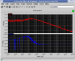
Here i have upload the ac, dc and transient response that i get..bt for the DC response it does not show any waveform...and transient response oso very weird..
for ac oso is the incorrect expected result..it should be low pass for lower frequency..

ac.PNG

dc.PNG

trans.PNG
 

Hi jlim,

1. You probably haven't corrected the the diode connection for NM3. The drain (ibias net) must be connected to the gate of the transistor.
2. Then you have to reverse the polarity of the idc source.
3. The OTA circuit has a Vdd node while at your testbench you have Vddd. Use Vdd here as well.
4. It is better if for your Vdd you connect the (-) of the vdc source to gnd (analogLib)
5. For your Vss do the same as for Vdd but instead use a vdc source with 0 dc voltage. Or use gnd in your OTA cell.
6. When I say annotate the DC operating points and Node voltages I mean Results -> Annotate -> DC operating points / DC node voltages.

Do 1 thru 5, and if it still doesn't work correctly, do 6 and post a screenshot of the OTA.

And also 60mA of current is too much for such a small transistor.
Try something in the range of ~10uA.
 
  • Like
Reactions: jlim

    jlim

    Points: 2
    Helpful Answer Positive Rating
thanks your reminder that there has lost of drain to gate connection for Ibias and also reverse polarity idc source..
but i try the value in range of ~10uA...the ac response is also weird the waveform seem like has the noise/disturbance..
for the annotate DC operating point and node voltages..i gt try it...But i when i click Result->Annotate, the DC operating points/DC node voltages cnt to be click on..
here i attach the ac response that i try for ibias=100pA...but the result is still incorrect...

new.PNG

n1.PNG

n2.PNG
 

for the annotate DC operating point and node voltages..i gt try it...But i when i click Result->Annotate, the DC operating points/DC node voltages cnt to be click on..

You must run a DC analysis in order to enable the annotate DC option. Give it a try.
 

i have try to run a DC analysis but it still cnt annotate DC option...even the DC response waveform also cnt show~~~ :(
 

thanks to teach me..
i have try it..here i attach the DC operating point and DC node voltage..
for idc i set 10nA..

dc pt.PNG
 

hello jlim, you're welcome.
The think is that you should know these stuff. There are many cadence tutorials at the internet for you to llok at.

You haven't done like I told you at post #14. Replace all vss (everywhere, top level and OTA) with gnd so that you have a ground at 0 volts.
And then I need the screenshot of the OTA at transistor level, like in post #11 but with the DC values annotated in order to help you, this top level image doesn't help to debug your circuit.
 

Status
Not open for further replies.

Part and Inventory Search

Welcome to EDABoard.com

Sponsor

Back
Top