Continue to Site
Follow along with the video below to see how to install our site as a web app on your home screen.
Note: This feature may not be available in some browsers.
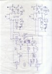
Kindly give information in detail for what changes need to be done for good and effective non-problematic battery charging. My experience with the original circuit is battery bulging due to overchargeI noted that many members have complain regarding charging.
I think method you are using is ok.
Just keep MCU pins low (which are switching lower fets for charging).
But remember primary volts are 7.
For your modified circuit,we need here 10.5v.
And we also need extra turns in secondary winding,to get optimal watts in inverter mode.
Original circuit?Kindly give information in detail for what changes need to be done for good and effective non-problematic battery charging. My experience with the original circuit is battery bulging due to overcharge
215 means 4.2v(charging cut off) at pin 3 of MCU.movf BATTV,w
sublw .215 ;CHG CUT OFF
btfsc STATUS,C
Where you read that, this code have trickle charging in it?method of frequency is the best,but constant current at 13.8v & after trickle is wrong.
can anybody change this charging system?
i am still waiting of pcb since last year.pnjbtr did you get good result after making changes in the ckt as you mansion above
can anybody adjust IR2110 with fet drive.
its is the best
i used,but not running succesfullyDo you mean that you want to change the gate drive circuitry so that IR2110 can be used?
Pin 7 of IR2110 is for high side fet, and pin 1 is for lower fet.Please check it
Yes. Look here!Pin 7 of IR2110 is for high side fet, and pin 1 is for lower fet.
Pin 5 is for high side return path.
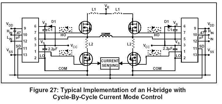
Some problems are being faced by us in connecting the IR2110 module to the PORTS,such as OSC1.OSC2,OSC3,OSC4 ,The problem is that the voltage level on these PORTS is insufficient to drive the IR2110 in perfect mode.
When the voltage were measured,approxmately 0.4 volts were present on each port.
At this moment,I am unable to understand that how I can increase the voltage level on these
PORTS,as you know, there are no pull up resistors on these PORTS.Can I add the four resistors on these PORTS like 4.7K etc ?
Another solution is that these changes canbe made in the Software,I mean,in the assembly file.Can you aggreed for this solution ?
At inverter mode or charging?When the voltage were measured,approximately 0.4 volts were present on each port.