Continue to Site

Welcome to EDAboard.com

Welcome to our site! EDAboard.com is an international Electronics Discussion Forum focused on EDA software, circuits, schematics, books, theory, papers, asic, pld, 8051, DSP, Network, RF, Analog Design, PCB, Service Manuals... and a whole lot more! To participate you need to register. Registration is free. Click here to register now.

How do I convert a patch antenna in HFSS to a PCB?

Status
Not open for further replies.

DeboraHarry

Full Member level 5
Joined
Dec 3, 2011
Messages
274
Helped
48
Reputation
94
Reaction score
43
Trophy points
1,308
Location
UK
Activity points
3,905
Assuming I designed a microstrip antenna, filter, coupler or simular, and drew and simulated it in HFSS, how could I take that to get a PCB produced by a commerical PCB manufacturer?

Any suggestions for UK PCB manufacturers that can produce boards on Rogers or similar laminates at sensible prices?
 
Last edited:
you can export every layer of your design to dxf format which is recognized by almost all pcb drawing packages.
 
So if there was two layers of copper, with a dielectric in between, would I export all three layers, or just the two copper ones?
 
You will have to create a Gerber (using CAM 360 or similar softwares) for the PCB guy to take into production.

As Amihomo says, few guys may entertain DXF as well but atleast here in India, we usually give gerber formats to pcb manufacturers.
 

You will have to create a Gerber (using CAM 360 or similar softwares) for the PCB guy to take into production.

As Amihomo says, few guys may entertain DXF as well but atleast here in India, we usually give gerber formats to pcb manufacturers.

What's CAM 360? A Google found me nothing on it. I also tried "CAD 360", on the off-chance you had mis-spelled what you intended, but that did not bring me anything useful either.

Ideally I'd use Linux software - open source would be even better. But anything that can permit me to output HFSS to a format I can easily get a PCB made. From what people are telling me, I need to output DXF first, which is fine, but I'd like some advice on a reliable, but economic solution. I don't want to spend a fortune on PRO E or similar, just to convert a file from one format to another.

Deborah
 

two methods are known to me:

1. export the .dxf file of your design layerwise, as in if there are two stacked dielectrics with two patches, you need to create two layers for these patches and so on. Next there is a software named (if i am not wrong in remembering its name) as Circuit Cam,which can create files suitable to machine etching process.

2. Create the layout of each of your layer (as in those having patches) using Correl Draw of any other CAD software that produces exact dimensions that you give. Next take its print out on a butter paper. Take it to manufacturer, they will turn it to a plastic film which would be impressed on your substrates and sides where copper is desired can be kept covered while where copper is not required can be exposed to the etchant.

these two methods are very well used at my institute in India, don't know about these facilities at your place.

Hope it helps.

Regards

Ashish

- - - Updated - - -

What's CAM 360?

may be he is referring to Circuit CAM only..
 
two methods are known to me:

1. export the .dxf file of your design layerwise, as in if there are two stacked dielectrics with two patches, you need to create two layers for these patches and so on. Next there is a software named (if i am not wrong in remembering its name) as Circuit Cam,which can create files suitable to machine etching process.

I was looking at one dielectric layer, with copper top and bottom. So do I need to export 3 layers in total?

2. Create the layout of each of your layer (as in those having patches) using Correl Draw of any other CAD software that produces exact dimensions that you give. Next take its print out on a butter paper. Take it to manufacturer, they will turn it to a plastic film which would be impressed on your substrates and sides where copper is desired can be kept covered while where copper is not required can be exposed to the etchant.

I think I'd prefer the first one. Firstly it is less error prone, and secondly there are places where one can just email/upload a file, though I don't have much idea about who to use for a Rogers or similar laminate. I've seen places do it very cheap, but I guess that's on FR4. I suppose it would be worth getting one made on FR4, even if it does not have the electrical characteristics I want, just to prove it before committing to a more expensive board.

I have a friend with a CNC mill, but he has only just got it, and so it not in a position to produce PCBs yet. I'm told that is more reliable, as the edges are sharper than with etching, though I don't know how true that is. The CNC milled PCBs I've seen are not too impressive, but that might be due to blunt/inappropriate tools, or operator error.

- - - Updated - - -

two methods are known to me:

1. export the .dxf file of your design layerwise, as in if there are two stacked dielectrics with two patches, you need to create two layers for these patches and so on. Next there is a software named (if i am not wrong in remembering its name) as Circuit Cam,which can create files suitable to machine etching process.

I was looking at one dielectric layer, with copper top and bottom. So do I need to export 3 layers in total?

2. Create the layout of each of your layer (as in those having patches) using Correl Draw of any other CAD software that produces exact dimensions that you give. Next take its print out on a butter paper. Take it to manufacturer, they will turn it to a plastic film which would be impressed on your substrates and sides where copper is desired can be kept covered while where copper is not required can be exposed to the etchant.

I think I'd prefer the first one. Firstly it is less error prone, and secondly there are places where one can just email/upload a file, though I don't have much idea about who to use for a Rogers or similar laminate. I've seen places do it very cheap, but I guess that's on FR4. I suppose it would be worth getting one made on FR4, even if it does not have the electrical characteristics I want, just to prove it before committing to a more expensive board.

I have a friend with a CNC mill, but he has only just got it, and so it not in a position to produce PCBs yet. I'm told that is more reliable, as the edges are sharper than with etching, though I don't know how true that is. The CNC milled PCBs I've seen are not too impressive, but that might be due to blunt/inappropriate tools, or operator error.
 

The standard international format is Gerber for production. DXF, etc can be used as well if your PCB guy can do it !

If you are looking for a very cheap solution and a simple design (1-2 layer), here it is!
1. Make a CAD drawing
2. Print the negative on a butter paper
3. Iron the butter paper on the substrate you intend to etch.
4. In case you want the ground plane, tape it before you etch it.
5. Once the print is on the substrate, you may put it in Ferric Chloride powder + warm water.
6. Stir for 20-30 minutes depending on the concentration of Ferric Chloride and make sure you dont over etch it.
7. Wash with plain running water.
8. Clean the substrate with Acetone.
9. Connect the connectors / cables /etc.
10. Your PCB is ready for testing.
 

the machine etching method works well with comparatively thicker substrates, and personally i used 1st method for FR4 only while i used 2nd method while fabricating the antenna structure of mine with RT duroid of around 10 mils thickness (quite less). The accuracy again depends on how you are familiar with working with the respective softwares.

as far as your single substrate query is concerned, even if your are using 1st method by machine etching, u need to export only one layer i.e. of your patch design and not the gnd plane. For ensuring that ground is not etched in both the methods is the responsibility of designer itself.
You need to mention that lower face of substrate be covered for 2nd method to avoid its etching.

Can i ask you the thickness of your Rogers substrate?

- - - Updated - - -

The standard international format is Gerber for production. DXF, etc can be used as well if your PCB guy can do it !

If you are looking for a very cheap solution and a simple design (1-2 layer), here it is!
1. Make a CAD drawing
2. Print the negative on a butter paper
3. Iron the butter paper on the substrate you intend to etch.
4. In case you want the ground plane, tape it before you etch it.
5. Once the print is on the substrate, you may put it in Ferric Chloride powder + warm water.
6. Stir for 20-30 minutes depending on the concentration of Ferric Chloride and make sure you dont over etch it.
7. Wash with plain running water.
8. Clean the substrate with Acetone.
9. Connect the connectors / cables /etc.
10. Your PCB is ready for testing.


Yes, obviously, this method is very common. But, i always prefer to get the process from step 3 onwards from the manufacturer, as substrates like RT duroid are quite expensive and the accuracy of etching is utmost important, which usually can not be attained easily by yourself at your labs.
Well, this method is really helpful in the circuit designing.

If you could afford a Laminator and a UV source, you could yourself do a great job as the printing on PCB is most critical for accuracy.
... and moreover in R&D, its pretty difficult and very time consuming to give the CAD design to manufacturer and wait for a week or so to get the samples.
 

If you could afford a Laminator and a UV source, you could yourself do a great job as the printing on PCB is most critical for accuracy.
... and moreover in R&D, its pretty difficult and very time consuming to give the CAD design to manufacturer and wait for a week or so to get the samples.

You just reiterated my words.
Even in R&D, there are special designated people who carry out these tasks.
 

The standard format for sending PCB layout for manufacturing is Gerber RS274X for the layout files and Excellon for the drill files, but those PCB manufacturers who support Rogers substrates usually accept DXF as well.

A few notes on DXF:
- Unlike Gerber, DXF can have many layers in one file. There is no need to split the layout into many DXF files.
- The DXF file should include the metal layers, drill layer(s) and a board outline layer.
- DXF layouts do not have units, so make sure that you cearly specify the drawing unit that you have used.
- DXF does not have area fill. The very widely used method for area fill is to have a closed polyline boundary.
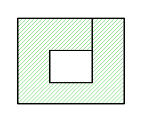
- DXF does not support anti-metal. If you have an area with a cutout, the hole must be implemented like this:
29_1345118797.png


It's a good idea to also include a document that shows a screenshot/print of your layout,
so that misunderstanding about metals/cutouts can be avoided.
 

Status
Not open for further replies.

Part and Inventory Search

Welcome to EDABoard.com

Sponsor

Back
Top