Continue to Site

Welcome to EDAboard.com

Welcome to our site! EDAboard.com is an international Electronics Discussion Forum focused on EDA software, circuits, schematics, books, theory, papers, asic, pld, 8051, DSP, Network, RF, Analog Design, PCB, Service Manuals... and a whole lot more! To participate you need to register. Registration is free. Click here to register now.

Problem with Voltage reference of ADC

Status
Not open for further replies.

chandra3789

Member level 1
Joined
Jun 11, 2011
Messages
36
Helped
0
Reputation
0
Reaction score
0
Trophy points
1,286
Location
kharagpur
Activity points
1,622
Hi friends..
i have a big problem with the reference voltage which i have to supply to the pipelined ADC, i have designed, on chip.I have generated the two reference voltages 1.3 and 0.5 Volts(with a common mode voltage of 0.9 V) through low voltage band gap reference circuit. I have to supply these two voltages to the ADC through a unity gain buffer. All is well until here. When i supply the reference to the ADC, large currents are being drawn from the references by the ADC because of which the voltage is changing rapidly. The reason for this is the references may have to drive large capacitance at clock edges depending upon the digital outputs. The requirement for the circuit is the reference has to be very steady even though large currents (upto 6mA) are drawn from it otherwise the performance of the ADC will be severely affected. I have tried many possibilities like using regulators, decoupling capacitors etc. none of them solved the issue. I also have a plan of supplying the reference off chip but the bond wire inductance will exacerbate the problem. So, please suggest me what should i do?....waiting for replies.....
 

What kind of amplifier are you using for the unity-gain buffer? It seems that the output impedance of your buffer is too high.
 

Reference voltages generally would be connected to points which dont draw current or very little. I suspect something is wrong in pipeline architecture/implementation.

if you need to pull 6mA out of your reference then you need regulators with that drive capability.
 

There are a few ways to handle the problem but we need more information. What frequency are you sampling at? What is it about the 6 mA current causing you a problem - is it a spike or a current that needs to be delivered through the whole sample period? Is the load signal dependent? How many bits?

If you use an external reference you will have to construct and RLC network to critically damp any oscillations caused by the bond wire inductance.
 
Last edited:

Reference voltages generally would be connected to points which dont draw current or very little. I suspect something is wrong in pipeline architecture/implementation.
Unless the reference voltage is connected to one (or more) capacitor(s) as in a switch-cap pipeline ADC. In this case, at every clock cycle, the reference needs to settle to its correct voltage.
As RobG mentioned, we need a bit more details on the implementation.
 

Unless the reference voltage is connected to one (or more) capacitor(s) as in a switch-cap pipeline ADC. In this case, at every clock cycle, the reference needs to settle to its correct voltage.
As RobG mentioned, we need a bit more details on the implementation.

Agreed. A schematic drawing would sure be of helpful to debug.
 

Yeah , let me give more details......
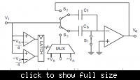
first of all the architecture i am using is a pretty standard one.it is shown below

in the circuit switch S3 connects capacitor Cs to either Vref+ or Vref- or VCM(0 without common mode voltage). The selection of the mux will be based on the output of the comparators. The mux is implemented using switches(transmission gates) and basic logic gates. The pipelined ADC i designed is of 10 bit resolution , sampling at 100 MHz . The ADC consists of 8 1.5 bit per stage stages each resolving 1 effective bit and a 2 bit flash ADC at the end which gives 2 LSB bits. Now when i supply the reference to the circuit , during switching action the capacitor may get connected to one of them. Because of that peak currents are drawn from the reference to charge or discharge the capacitor Cs. While those currents are drawn from the references the reference voltage is changing rapidly. I think there is no other efficient implementation of the mux which prevents current requirement.......

waiting fot your replies.....

---------- Post added at 13:43 ---------- Previous post was at 13:39 ----------

First of all is it a good idea to supply reference externally?
 

You can sample your input at that speed/accuracy, so you can sample a reference too. You need to damp the ringing from the bond wire with a suitable RC combination. The R needs to be small enough that the IR drop is acceptable, especially since the load on the reference will depend on the code for that topology. It will help if you can make the load independent of the signal, but at 10 bits you can probably get away with the topology you've chosen. Since you asked (and were not told by your boss) I assume you are doing this for research work, not industry. In that case I'd use an external reference just to limit the number of things that can go wrong.

You can limit the size of the current spike by using more resistive switches. I think if you are clever you can choose the size of each switch to critically damp the signal to each capacitor.

If you want to buffer the voltage internally you have two main options: 1) a very fast buffer that recovers as fast as your main amplifier, 2) a very slow amp with a very large cap at the output. It will be a disaster if your buffer speed is in between, which is probably where you are now. The problem with 1) is that it takes a of of current. The problem with 2 is that it looks like a relatively large resistance unless you burn a lot of current and use a large filter capacitance.

You can also use a source follower. The key to that is providing a reference that is 1 Vgs too high, and then connecting the gate of your source follower to that node.
 

It seems that you are using a very standard MDAC topology. The reference buffer must be fast enough to recover from the glitches at every clock cycle and therefore you need to use more current (try doubling the size of your unity buffer).

For a 100MHz ADC you could also use an external reference (especially if it is academic work - you can save on the power consumption numbers!) as RobG mentioned. Consider double bonding to decrease the inductance and use a big on-chip capacitor.
 

I have a problem with the common voltage for a sigma delta ADC. The sample frequency is 4MHz, but this common voltage presents many glitches. What would be your recommendation for designing the buffer that I need for this common voltage reference? what architecture should I use? the buffer needs a higher frequency than 4Mhz?? it is necessary to use an external capacitor?? the common voltage is 1.2V.

thanks in advance
 

Before looking into the buffer, check your clock timing. Glitches might be created by (dis)connecting the capacitors at the wrong time. As a side note, the bandwidth of the buffer should be larger than 4MHz but be aware that if it is too wide it might allow too much noise.
 
  • Like
Reactions: jc2

    jc2

    Points: 2
    Helpful Answer Positive Rating
What architecture would you recommend me for using? a simple differential pair with a CLASS AB output stage?

when you say that the bandwidth of the buffer should be larger than 4MHz, you are referring to the complete buffer (I mean the gain stage with the output stage) or only to the output stage?

thanks
 

What architecture would you recommend me for using? a simple differential pair with a CLASS AB output stage?
It depends on your requirements. Sometimes a simple differential pair is enough, sometimes you need a more complex amplifier. If you are driving a capacitive load only, a folded cascode op-amp would probably work well.
when you say that the bandwidth of the buffer should be larger than 4MHz, you are referring to the complete buffer (I mean the gain stage with the output stage) or only to the output stage?
The bandwidth of the amplifier should be large. When you close the loop you need to have a good response.
 
  • Like
Reactions: jc2

    jc2

    Points: 2
    Helpful Answer Positive Rating
To implement this circuit, you should describe the input signal in details.
 

Status
Not open for further replies.

Part and Inventory Search

Welcome to EDABoard.com

Sponsor

Back
Top