Continue to Site

Welcome to EDAboard.com

Welcome to our site! EDAboard.com is an international Electronics Discussion Forum focused on EDA software, circuits, schematics, books, theory, papers, asic, pld, 8051, DSP, Network, RF, Analog Design, PCB, Service Manuals... and a whole lot more! To participate you need to register. Registration is free. Click here to register now.

driver for power mosfets of 1 kV half bridge power supply

Status
Not open for further replies.
Hello, thank you very much for the comments!

Another try, here is the schematic:
HB2.jpg
If that doesn't work, here is another link:
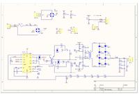
ta-daaaa

Thanks mtwieg for pointing out the fact that the transistors are getting warm with low power at the output. Maybe it's necessary to tune better the snubber network. I know the -first- gate circuit was terribly bad!, that's because I've started the thread. The second one, is in the schematic here uploaded, and also tested. I don't know if it's soooo bad. I tried to copy one from a atx power source.

Yes you're right with the topology, I didn't use the forward converter because the power transformer has 3 windings. I thought it's more difficult to calculate and to build that transformer than the drive circuit. But, oh well, now I'm stuck with this.
And in the flyback, not sure, but I've read that the max voltage across the transistor is Vin+Vout×(Np/Ns) = 311+1000*0.25=561V, plus the overshoot, to me it was like to much voltage.

Well, didn't have time to try anything yet. I'll try the gap on the power transformer(pot core from epcos) and tune better the snubber network. Not sure what to do with the gate driver.

Best regards to all, have a nice time, bye!
 

Hi again
Thanks mtwieg for pointing out the fact that the transistors are getting warm with low power at the output. Maybe it's necessary to tune better the snubber network.
How much dead time did you create ? perhaps it isn't enough .
And about ferrite transformers : no they are not difficult . try to be friend with them ! those are my best friends . you should learn easy way to talk with them !
See below , please :
https://www.edaboard.com/threads/229615/
Best Wishes
Goldsmith
 
Last edited:

Hi again
How much dead time did you create ? perhaps it isn't enough .

In the TL494, isn't there a dead-time forced by hardware??, I don't remember, it was something about 10% of duty cycle?

Thank you for the notes about ferrites, I'll read them carefully. Very nice, thanks!!


Regards!
 

In the TL494, isn't there a dead-time forced by hardware??, I don't remember, it was something about 10% of duty cycle?
Hi again
For dead time , see the duty of pin 4 of your IC , and another thing , about mosfets that you used : try to change your mosfets with another mosfets with lower ciss .
Best Wishes
Goldsmith
 

Another try, here is the schematic:
View attachment 71422


Thanks mtwieg for pointing out the fact that the transistors are getting warm with low power at the output. Maybe it's necessary to tune better the snubber network. I know the -first- gate circuit was terribly bad!, that's because I've started the thread. The second one, is in the schematic here uploaded, and also tested. I don't know if it's soooo bad. I tried to copy one from a atx power source.
Now I have no idea what you're trying to do with your gate drive, especially with the RCD network on the secondaries. Are you sure those capacitors aren't supposed to be resistors? And that 220 ohm resistor on the primary is still going to severely cripple the gate waveforms.

If you want to just copy a gate drive circuit from somewhere, try this: **broken link removed**
The circuit in figure 39 is good enough for your application. Since the TL494 doesn't have totem pole outputs, you should use a center tapped primary like you have in your schematic (but the series resistor isn't necessary and will just hurt performance).
And in the flyback, not sure, but I've read that the max voltage across the transistor is Vin+Vout×(Np/Ns) = 311+1000*0.25=561V, plus the overshoot, to me it was like to much voltage.
That's the case with a typical single switch flyback. The two switch/diagonal flyback clamps the switch voltage to the input DC voltage.
 

Thanks mtwieg!

I know it looks weird the gate driver. It's based on the gate drivers from atx power sources. If you search for schematics of 300W atx power sources with half brigde, you will find something very similar.
Plus, I found this page very usefull, check it out!

https://w5jgv.com/hv-ps1/

This guy has done a pretty well job. I've used much things from there.

The app note you passed looks great, I'll read it all. Thank you very much!

best regards!
 
Which schematic in particular are you referring to? I clicked on a few and none of them show what you have.

And just for the record, ATX power supplies aren't the best source of information. They generally work, but they're designed for cost efficiency alone, and they cut a lot of corners in the designs (using logic gates as comparators, for example...).
 

The gate drive in that ATX schematic is nothing like yours. They don't have any resistor on their primary. And no capacitors on the secondary. Their schematic looks fine (though you probably don't need something so complicated).
 

Right, it's complex, that's why not used exactly that, but something seen in atx schematics as mentioned earlier, to do the same trick.
The good of that page is that explains very well what does each component, and the possibly problem on each function. It helped me to be aware of potencial problems I didn't know.

The idea with the gate driver used is:
* Block oscillations during on time. The positive pulse from winging puts diode on direct pol., and cap charged.
* Discharge quickly the gate on off time. The diode gets on reverse pol, and the gate charge finds a path trough the capacitor, the 1ohm resistor and winding.
 

Dear arkanwe
Hi
Thank you for the link at post #26 . it is interesting for me , and i think it will be interesting for all of the peoples that are interested at SMPS .
Best Regards
Goldsmith
 

Dear arkanwe
Hi
Thank you for the link at post #26 . it is interesting for me , and i think it will be interesting for all of the peoples that are interested at SMPS .
Best Regards
Goldsmith

Great!, I'm glad it helped you.


I've checked the resistor in series with the center tap of the driver transformer. With a resistor of 10 Ohm works OK!.

Now rests check the snubber network, the transformer design and gap. And try to improve the gate driver.

Thanks to all!
 

Dear arkanwe
Hi again
It is a suggestion , you can accept or not ! why not using an optocoupler for driving mosfets ( it is more linear than transformer and cheaper and compact , e.g 6n136 , which has a totem pole internally at the out put ! )
Best Wishes
Goldsmith
 

Dear arkanwe
Hi again
It is a suggestion , you can accept or not ! why not using an optocoupler for driving mosfets ( it is more linear than transformer and cheaper and compact , e.g 6n136 , which has a totem pole internally at the out put ! )
Best Wishes
Goldsmith

Thats a good suggestion. To think about.
As the smps is switching at 200 kHz, I've thought the optocoupler would be too slow. To be sure tested the 4N25, which is the only one I can buy around here. And didn't worked fine at 200kHz.
I've used the transformer because almost every half bridge around there used something like that.

It would be really interesting to make this smps with the optocouplers. I think I'll try that for the next design, and for now to see if this one can work.
 

I used 6n136 at 250KHZ , and one of my friends used it for 1MHZ transmitter . ( but i didn't use it for this frequency , but i'm surer about it's behavior at 250KHZ. however you can find many faster optocouplers simply)
Good luck
Goldsmith
 

Right, it's complex, that's why not used exactly that, but something seen in atx schematics as mentioned earlier, to do the same trick.
The good of that page is that explains very well what does each component, and the possibly problem on each function. It helped me to be aware of potencial problems I didn't know.

The idea with the gate driver used is:
* Block oscillations during on time. The positive pulse from winging puts diode on direct pol., and cap charged.
* Discharge quickly the gate on off time. The diode gets on reverse pol, and the gate charge finds a path trough the capacitor, the 1ohm resistor and winding.
Yes, oscillation is a concern because of the open collector push pull drive of the TL494. That's why a pulldown circuit like the one in the ATX schematic is needed. Your circuit has no such functionality, and the gate will oscillate. The capacitor in your gate drive circuit has no functionality as far as I can tell. I'm not sure what you think it is doing, especially since it isn't present in the ATX schematic.
 

Check this schematic

atxps.png

I've used a gate driver from an atx smps like that one, and followed the topology from the web page link from #28, just as a guide.
 
Last edited:

That schematic uses BJTs as switches, and thus there is much less risk of an oscillation. I'm not really sure what's going on with the rest of the gate drive circuit, the schematic is so terribly laid out. But it's obvious what they're doing won't apply to a converter built with FETs or IGBTs.
 

That schematic uses BJTs as switches, and thus there is much less risk of an oscillation. I'm not really sure what's going on with the rest of the gate drive circuit, the schematic is so terribly laid out. But it's obvious what they're doing won't apply to a converter built with FETs or IGBTs.

Dear mtwieg,
How would you drive the mosfets of a half bridge smps?
 

A gate drive transformer can work, when properly designed, though it's tricky due to the TL494's output structure; you need special pulldown circuits like those found in the first ATX schematics you posted. Otherwise you can get a gate drive IC with totem pole outputs, then you can use simpler gate drive transformers with no additional pulldown (like figure 39 of that TI document). Or you could get a bootstrapping high side gate driver, if you have access to them. I would go with the last option, myself.
 

Status
Not open for further replies.

Similar threads

Part and Inventory Search

Welcome to EDABoard.com

Sponsor

Back
Top