Continue to Site

Welcome to EDAboard.com

Welcome to our site! EDAboard.com is an international Electronics Discussion Forum focused on EDA software, circuits, schematics, books, theory, papers, asic, pld, 8051, DSP, Network, RF, Analog Design, PCB, Service Manuals... and a whole lot more! To participate you need to register. Registration is free. Click here to register now.

Efficient bottom feed for patch antenna array

Status
Not open for further replies.

GiedriusR

Newbie level 3
Joined
Feb 5, 2012
Messages
3
Helped
0
Reputation
0
Reaction score
0
Trophy points
1,281
Activity points
1,303
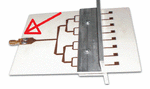
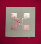
Hi, I am working on a 4x4 rectangular microstrip patch antenna array for my uni project and I can't find a proper way to feed the whole array. I have found that most of the people usually feed the whole array using a bottom insert feed, but whenever I try to do the same - CST simulation results show a very low S1,1 result. I have tested the design as well to check that simulation results are correct with no luck. Could anyone please recommend me a proper way of feeding a large microstrip array?
 

Hello GiedriusR

As far as the feed network is concerned, there is nothing wrong with the network unless, network has not been built properly. if you have mismatches in one section it builds up through out the system and leads to a poor reflection coefficients. on top of it your feed network pattern depends on how the power needs to be divided.

Hope that helps

Regards
Elchiquito
 

Thank you for your reply, elchiquito.

As far as the network is concerned - it is fine. I checked it using a feed input similar to one shown in figure 1 (attached image) and it proves to be quite efficient. What I am trying to do, is to design one bottom fed input to the system much like one shown in figure 2. The approach shown in figure 2 seems bringing the S1,1 value down by quite a lot. Could you please suggest any reason for that happening?

Note that both of the images are just representing the feeding method and is not my actual work.

Thanks for the help,

Giedrius
 

Attachments

  • Figure 1.gif
    Figure 1.gif
    18.6 KB · Views: 148
  • Figure 2.jpg
    Figure 2.jpg
    98 KB · Views: 140

The only Reason i can think of is that you are continuing with the same line width as of 50 ohms. since power is getting divided more in like a parallel circuit the width of the line should be 100 ohms. (100*100)/200=50 ohms, where you will get better reflection coefficient. let me know if it still doesn't make sense

Hope that helps

Regards
Elchiquito
 
That makes sense, I will alter the design. Thanks for your help, Elchiquito.

Regards,

Giedrius
 

Status
Not open for further replies.

Part and Inventory Search

Welcome to EDABoard.com

Sponsor

Back
Top