lufer17
Member level 5
Hello, I have a question regarding the manufacturing process of electronic components in the case of the silicon deposition and corrosion process. My biggest doubt is the behavior of the plasma interacting in the reactor, I don't know if it's correct I would like someone to help me.
What I understood from the subject:
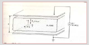
If you look at the image, it shows a capacitor (in the simplified case, a PECVD or RIE plasma reactor) where the particles descend from the plate and then it will collide with the particles on the bottom plate, in this case it is in the middle where the plasma wants to pass. In practice we have three directions (vectors) x, y and z, the magnetic effect occurs in the plasma where the particles have two directions or two directions in a spiral effect, so the shock is greater in the sample. In its behavior taking advantage where the field can move in the sample without having to move it.
Is correct?
What I understood from the subject:
If you look at the image, it shows a capacitor (in the simplified case, a PECVD or RIE plasma reactor) where the particles descend from the plate and then it will collide with the particles on the bottom plate, in this case it is in the middle where the plasma wants to pass. In practice we have three directions (vectors) x, y and z, the magnetic effect occurs in the plasma where the particles have two directions or two directions in a spiral effect, so the shock is greater in the sample. In its behavior taking advantage where the field can move in the sample without having to move it.
Is correct?