Continue to Site

Welcome to EDAboard.com

Welcome to our site! EDAboard.com is an international Electronics Discussion Forum focused on EDA software, circuits, schematics, books, theory, papers, asic, pld, 8051, DSP, Network, RF, Analog Design, PCB, Service Manuals... and a whole lot more! To participate you need to register. Registration is free. Click here to register now.

Receiver circuit, what does Q4 do?

Status
Not open for further replies.

dr pepper

Advanced Member level 1
Joined
Mar 15, 2010
Messages
420
Helped
34
Reputation
68
Reaction score
40
Trophy points
1,308
Location
lancs
Activity points
4,128
I understand this circuit for the most part, however not sure what Q4 does.
It looks like a reverse biased diode from +v the way its connected, is this an odd means of making a zener type regulator or something?
 

Attachments

  • radio.png
    radio.png
    204 KB · Views: 131
Last edited:

It is a reverse biased diode used as a reverse voltage protection for the NE602 circuit.
 

Seem like an odd way to protect the chip, I wonder why not put a reverse 1n4001 across the batt.
 

Diode connected Transistors are always in sat, and exhibit very low reverse leakage, not sure why latter
would matter in this circuit. Its also a more ideal log characteristic connected this way than a normal
diode.
 

Yes, it's working as zener diode.
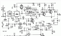
Something odd about circuit, the NE602 max Vcc 9V, the 2N3904 VBR(ebo) is min 6V,
so whats max Vbr(ebo) ? Whats it there for ? If to protect against excessive Vcc its not
a guarentee clamp < 9V to do so.

Just ODD.

Regards, Dana.
 

Yes it's odd. Typical EB junction zener voltage of silicon BJT is around 7 V at 1 mA, if I remember right.
 

So it is a power supply protection device for the mixer.
I've seen tranny junctions used as audio detectors that makes sense, not this.
Maybe the designer happened to have a sprinkling of 2n3904's on his/her bench at the time.
 

Erp take another look at this schem, as it wont work.
U2a pin 3 is obviously the audio in from the detector, but its grounded so there will be no audio.
I think the ground symbol on the junction of R11 & C13 is a mistake and should be omitted, or the lower link between them taken out.
Also think the + end of C17 should go to U2 pin 1, looks like its connected to the agc filter.
 
Last edited:

Is not a Zener.
Without any load (NE602 circuit) the voltage accross the Q4 transistor follow one-to-one the Vcc voltage.
Is just a simple reverse biased diode.

With normal 3mA current taken by the NE602 circuit, the supply voltage of the IC is about 8V (due to voltage drop on R5), so the circuit is protected from working to the 9V datasheet limit.
But from what I know, the normal operation of NE602 is at 6V.
 

the voltage accross the Q4 transistor follow one-to-one the Vcc voltage
You say, Vbr(eb) is considerable higher than stated above? I'm not sure, may be it is for some transistor types.
 

Here is a 2N3904 operating as Vz out of my junk box -

1618786604052.png


Regards, Dana.
 

    FvM

    Points: 2
    Very helpful
Looks like voltage regulation action, and linear.
The datasheet does say 6v.
 

Here is a 2N3904 operating as Vz out of my junk box
The Vbr level isn't indicated in the oscilloscope screenshot, I read it as 8V above trigger level, about11.2 V. I see a similar Vbr with BC237.

I'm however quite sure, that I have operated NPN BJT (I believe BC107) as noise diodes at lower Vbr. For the time being, I'd say, there's apparently a larger range of actual Vbr, clarifying that Q4 is effectively useless in the shown circuit.
 

The scope screen shot shows a Vbr of 8V. The point at which the ramp (V1) is clamped. 2N3904 configed
as a Zener to ground.

Vbr part to part, type to type, probably all over the map in variation as its not a screened datasheet value.

1618827339597.png


Regards, Dana.
 
Last edited:

O.k., I misinterpreted the screenshot. 8V is nearer to the typical values I have seen previously.

In fact Vbr(eb) is no datasheet parameter. You should also consider that operating a transistor as zener diode is said to degrade the performance, particularly current gain and noise figure.
 

Unless I misunderstoof on semi's datasheet says the base breakdown voltage is minimum 6v.
Doesnt really matter anyway the datasheet for the ne602 says I can just use a 1k from +9v as the chip has a zener in it.
 
  • Like
Reactions: FvM

Status
Not open for further replies.

Part and Inventory Search

Welcome to EDABoard.com

Sponsor

Back
Top