Continue to Site

Welcome to EDAboard.com

Welcome to our site! EDAboard.com is an international Electronics Discussion Forum focused on EDA software, circuits, schematics, books, theory, papers, asic, pld, 8051, DSP, Network, RF, Analog Design, PCB, Service Manuals... and a whole lot more! To participate you need to register. Registration is free. Click here to register now.

problem on buffer output load

Status
Not open for further replies.

Paul98

Member level 5
Joined
Sep 7, 2020
Messages
86
Helped
1
Reputation
2
Reaction score
0
Trophy points
6
Activity points
647
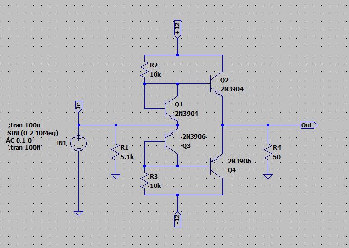
Hi ,i've drew this circuit.

10M.JPG


I have seen that the output wave is distorted as the value of the output load decreases, and obviously reducing the load also decreases the amplitude. Now this is a buffer where I would have expected better behavior under low loads but it didn't happen. Is there any way to limit this distortion and loss of amplitude? My first suspicion is that the transistor type are not suitable for low loads despite their Ft being covered. Thanks.

10MG.JPG


50MG.JPG


100MG.JPG
 

Solution
I would reduce the 10K resistors to the point that you
can make output crest voltage into Rload, while
demanding well less than peak beta. Parallel multiple
small transistors in the output legs or use bigger ones
(although this is inferior matching guaranteed). I'd put
a resistor between the "pilot" emitters and the "output"
emitters, value TBD, to keep the Vbe match tighter
under slewing conditions.

A Darlington approach would greatly relieve beta
sensitivity and maybe allow front end bias current
but you'll double the transistor count (though most
can be small).

Old timey transistor databooks from RCA, Motorola
et al used to have whole sections of application notes
and circuits for linear audio and MHz-range RF
amplifiers; they...
Hi,
Now this is a buffer where I would have expected better behavior

classical non feedbacked Class B behaviour. Quite expectable.

Where is this circuit from? Is it a reliable source of circuits with good documentation? Give a link.

Klaus
 
Look at your rbias/rload. That says you need a beta well greater than 10K/50=200 to not be bias limited.

Then consider that those transistors are small signal, not power types.

At high amplitudes your resistor bias will be fading at the maxima / minima just when you need the base drive most. This is a distortion actor and one reason for using current mirror racks in linear amps.
 
@KlausST

I did a google search and among the various forums and sites this scheme came out and replicated it on the spice. I can't tell you if it's a serious site or not because I don't have the technical knowledge to be able to judge it. Basically it works and as @dick_freebird wrote maybe the transistors are not suitable for this purposes. Do you have any idea what to use instead without completely changing the circuit?
 

I would reduce the 10K resistors to the point that you
can make output crest voltage into Rload, while
demanding well less than peak beta. Parallel multiple
small transistors in the output legs or use bigger ones
(although this is inferior matching guaranteed). I'd put
a resistor between the "pilot" emitters and the "output"
emitters, value TBD, to keep the Vbe match tighter
under slewing conditions.

A Darlington approach would greatly relieve beta
sensitivity and maybe allow front end bias current
but you'll double the transistor count (though most
can be small).

Old timey transistor databooks from RCA, Motorola
et al used to have whole sections of application notes
and circuits for linear audio and MHz-range RF
amplifiers; they used to make complementary discrete
NPN / PNP product pairs that they wanted to show
how to use. Might go scrounge for scanned copies.
 
Solution
OK. I hope to find copy of those books. I've lower resistor from 10k to 1k and on simulation seem to be solved. There's a possibility the transistor become hot?. Tomorrow i will try the other option. Thanks.
 

I can't tell you if it's a serious site or not because I don't have the technical knowledge to be able to judge it.
This is why you should look for a source with good explanations...not a tinkerer's play.
And this is why I asked for a link, so we can discuss about it.

Klaus
 

This is why you should look for a source with good explanations...not a tinkerer's play.
And this is why I asked for a link, so we can discuss about it.

Klaus
I agree , the web is full of a non sense circuits but sometimes with little you can get it to work and in the meantime you also get familiar with the simulator.. Anyway i done a search and found the link. As already said I don't yet have the technical knowledge to be able to judge the work of others, however the site seems serious to me.

SOURCE
 

Hi,

As already said I don't yet have the technical knowledge to be able to judge the work of others, however the site seems serious to me.
Indeed the site looks serious.

Even without much knowledge you should be able to judge such informations... in future
* The more detailed the better.
* If there are formulas and calcualtion examples --> better
* if you are interested in low distortion, but there is no information about distortion --> bad

What you maybe can´t judge:
* I miss the information that both upper transistors need to be thermally coupled. Best: glue them together.
* The same is with the two transitors at the bottom.
* They show step by step circuits with improvements. But they don´t clearly describe the improvement (why and how..), they don´t describe drawback, they don´t describe design considerations (thermal coupling)

Klaus
 
My first suspicion is that the transistor type are not suitable for low loads despite their Ft being covered.
Ft is the frequency where small signal current gain falls to unity. Comparing your 10 MHz and 50 MHz simulations shows that too low Ft respectively unsufficient bias current is exactly the problem.

For 50 MHz operation frequency, you either need a larger fT margin (using GHz transistors) or design for lower current gain. The circuit behaviour can be improved a bit by bypassing the diodes with small capacitors, e.g. 1 nF.

I've lower resistor from 10k to 1k and on simulation seem to be solved. There's a possibility the transistor become hot?
Surely. You should also consider that e.g. 5V magnitude relates to 100 mA current through 50 ohm resistor. A 50 ohm buffer involves some power dissipation anyway.

In most applications, the buffer would be supplemented with 50 ohm series termination, at least if it's intended to drive external loads. Otherwise it can easily become unstable with reactive loads or can be destroyed by short circuits.
 
I believe that one of the main purposes of the buffer is to allow low impedance loads to be used in a circuit that normally could not. In the case at the beginning of the discussion there are low power transistors therefore more than power buffer we could speak of interstage buffer. Obviously, modifying the components would change everything like already said.
 

Status
Not open for further replies.

Similar threads

Part and Inventory Search

Welcome to EDABoard.com

Sponsor

Back
Top