Continue to Site

Welcome to EDAboard.com

Welcome to our site! EDAboard.com is an international Electronics Discussion Forum focused on EDA software, circuits, schematics, books, theory, papers, asic, pld, 8051, DSP, Network, RF, Analog Design, PCB, Service Manuals... and a whole lot more! To participate you need to register. Registration is free. Click here to register now.

MOSFET heating problem

Status
Not open for further replies.

Anum72

Newbie level 4
Joined
Apr 10, 2012
Messages
5
Helped
0
Reputation
0
Reaction score
0
Trophy points
1,281
Activity points
1,326
Hi!
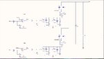
I am designing a shunt regulator which regulates the power from the solar panels. The power that is required by the loads is transferred from the solar panels to the loads and the extra power is dissipated through the shunt regulator unit. The circuit diagram is attached.
The comparator drives the MOSFET IRFZ44N (the datasheet is attached), when the bus voltage exceeds 28 volts the comparator gives high signal and MOSFET gets ON and extra power is shunted through the MOSFET.
Vsupply=12V
My problem is the MOSFETS are getting hot. The comparator having higher Vref (28.1V) gives pwm signal which is given at the gate. The pwm driven MOSFETS are getting hot. The comparator having Vref=28V gives ON signal that is 12V and its MOSFETS are not getting hot. Please help me out in finding the reason why the MOSFETS are getting hot. If anything related to the circuit is not clear please ask. Your help will highly be appreciated.
Thanks.
 

Attachments

  • 2Sections.JPG
    2Sections.JPG
    69.3 KB · Views: 183
  • irfz44n-2.pdf
    104.3 KB · Views: 88

You must quick charge and disharge capacitenca on FETs gate:
https://en.wikipedia.org/wiki/Gate_driver

It is often stated[by whom?] that transistors such as MOSFETs with isolated gate electrodes can be driven without a power source, which is not correct. In contrast to bipolar transistors, MOSFETs do not require constant power input, as long as they are not being switched on or off. The isolated gate-electrode of the MOSFET forms a capacitor (gate capacitor), which must be charged or discharged each time the MOSFET is switched on or off. As a transistor requires a particular gate voltage in order to switch on, the gate capacitor must be charged to at least the required gate voltage for the transistor to be switched on. Similarly, to switch the transistor off, this charge must be dissipated, i.e. the gate capacitor must be discharged.
 
  • Like
Reactions: Anum72

    Anum72

    Points: 2
    Helpful Answer Positive Rating
I have designed a gate driver for MOSFET IRF640 that is used for 220VDC universal motor speed control.
M75Py.png

This is gate drive circuit , Original circuit is little bit different Because later i added some di/dt and dv/dt protection.
You should use gate drive methods to provide sufficient power to the MOSFET's gate terminal.
 
  • Like
Reactions: Anum72

    Anum72

    Points: 2
    Helpful Answer Positive Rating
Thanks. I will try this gate driver, what should be the values of Rgate and resistor at the base of BJTs?
 

I have designed the circuit as mentioned in post#3, but the mosfets are still getting too much hot. Please provide the original circuit that contains di/dt and dv/dt protection.

The mosfets are damaged after getting too much hot. Also if the single mosfet is used to dump the extra power, it is not getting hot But if two parallel mosfets are used then the mosfets are getting too much hot. Why is it so? Is there any alternate method to dump the extra power of the solar panels?
 

Unfortuanately none of the previous contributors seems to understand the problem of your design.

It's quite simple, you are designing a linear shunt regular which can't but dissipate the unwanted solar panel power in the transistors. You can partly reduce the transistor power disspation by placing a series power resistor that shares most power in the upper range. The total dissipated power will be the same, but resistors can tolerate higher temperatures. Or use a different concept than shunt regulator.
 
  • Like
Reactions: Anum72

    Anum72

    Points: 2
    Helpful Answer Positive Rating
You can partly reduce the transistor power disspation by placing a series power resistor that shares most power in the upper range. The total dissipated power will be the same, but resistors can tolerate higher temperatures.


We have used power resistors in series with the MOSFETS (R1,R2, R9 and R10) that are not getting hot. Where else we can place the series power resistors?
 

Attachments

  • 2Sections.JPG
    2Sections.JPG
    69.3 KB · Views: 132

Your schematic is missing some info.
Why is their PWM on lower array? Is this not due to hysteresis of pot controlled positive feedback causing a relaxation oscillator dependant on Pot position.

The switching threshold will not be 28 or 28.1 since the hysteresis of positive feedback will raise and lower the sensed Vbus by at least 20% of Vs from R divider ratio on (+)

How can you supply LM358 with 12V and feed inputs at 28V? (NG!) Scale your input voltages down.

Your circuit does not show batteries or load, so I assume they are both the same (Load) and thus you have a "low-side" switched PV to load circuit not a shunt overvoltage circuit. It just enables the PV when there is sufficient voltage with hysteresis.

If your power resistors are equivalent to 50 mΩ @ 75W and your two MOSFETS are equivalent rated at 17.5 mΩ with Vgs=10 thus you have equivalent switch at ~9 mΩ

The power dissipation in the MOSFETS compared the series resistors is proportional to the resistance ratio since they share the same current. Thus if the 75W resistors are dumping 50 W, the MOSFETS are dumping 9 W. This requires a heat sink.

The complementary emitter follower is one way to lower the gate driver impedance to improve gate capacitance RC turn off time which can reduce dynamic switching losses greatly.

Also faster switching means increasing di/dt and EMI issues if you did not plan this carefully. Twisted power cables may help some with torroidal common mode core.

Many other improvements could be made such as cap across PV panel to regulate noise and improve MTTP using 75% of no load voltage for optimal battery or load.

In summary, reduce hysteresis with bigger R ratio, fix Vs issue on LM358
 
  • Like
Reactions: Anum72

    Anum72

    Points: 2
    Helpful Answer Positive Rating
Thanks all for your help. I have tried the gate driver circuit by using 7406 schimmit inverter, now the MOSFETS are not getting hot.

The next step is to design DC bus capacitor bank which I have shown in the schematic as C3. The purpose of this capacitor bank is to remove the ripples and provide constant 28V at the bus. I have got this formula to calculate the capacitance value;the peak to peak ripple output voltage is given as,
Vpp= Isc*Rc + (D(1-D)*Isc)/(C*fs)
if D=0.5,
Vpp= Isc*Rc + (0.25*Isc)/(C*fs)
so, the capacitance is calculated as,
Cmin ≥ (0.25*Isc)/((Vpp-Isc*Rc)*fs)
where,
C= capacitor bank value
fs= PWM switching frequency
Vpp= maximum ripples at the output before the capacitor
Rc= ESR (Equivalent series resistance) of the capacitor
Isc= short circuit current of the solar panels or the current that is shunting
Here, Isc and Vpp are known but I am confused about the values of fs and Rc as the switching frequency (fs) of the PWM is changing as the load changes. Please tell me any method to determine the value of capacitor bank.
Thanks.
 

Status
Not open for further replies.

Similar threads

Part and Inventory Search

Welcome to EDABoard.com

Sponsor

Back
Top