Continue to Site

Welcome to EDAboard.com

Welcome to our site! EDAboard.com is an international Electronics Discussion Forum focused on EDA software, circuits, schematics, books, theory, papers, asic, pld, 8051, DSP, Network, RF, Analog Design, PCB, Service Manuals... and a whole lot more! To participate you need to register. Registration is free. Click here to register now.

Interchangeable multiple analog IO

Status
Not open for further replies.

michcfr

Advanced Member level 4
Joined
Mar 7, 2012
Messages
106
Helped
0
Reputation
0
Reaction score
0
Trophy points
1,296
Activity points
2,011
Hello,
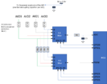
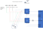
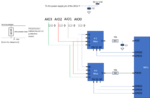
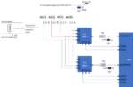
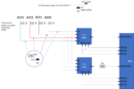
I want to add flexibility for analog IO to my MCU that has a single ADC (also usable as PWM) and a single PWM (also usable as ADC).
Requirements that drives my solution:
-4 analog IO ports (AIO0, AIO1, AIO2, AIO3) used interchangeably as ADC or PWM
-only two IO ports can be used at once

My solution use two 4:1 analog mux/demux driven by the MCU. See the schematics.
-one 4:1 mux/demux is used for the ADC line and the other one for the PWM line
-the two 4:1 mux/demux are driven by the GPIOs of the MCU. Maybe the GPIOs for EN are useless?

Can you please review my solution: is it correct? Improvement? alternative solution?

Thank you
Michel

schematics.png
 

Hi,

surely possible.
The ADC MUX does not need EN, becausser there can be no short circuit condition.

But the AIOs can be driven externally and in case the PWM MUX drives the same line, then there will be some short circuit.
You may use a series reistor to prevent damage.

I generally add an RC filter to the ADC inputs. As noise filter and as anti aliasing filter.
If the AIOs (or any other signals) leave the PCB than I always add some ESD protection.
And every supply pin of every IC gets a fast decoupling capacitor.
Deselected (PWM) AIOs are left floating. I general recomendation is not to leave any signal floating. (neither digital, nor analog)
You call it analog, but PWM is purely digital.

Be careful not to overdrive the ADC input with full swing PWM signals or external signals.

May I ask why not get best flexibility by 4 ADC inputs and 4 PWM outputs?

Klaus
 

Thank you KlausST for your advices.
According to your remarks I have changed the design. See the picture. Is it correct ? Sorry if there are trivial mistakes, I'm a beginner in eletronics.
Any idea on how to manage floating deselected (PWM) AIOs?

May I ask why not get best flexibility by 4 ADC inputs and 4 PWM outputs?
Because the PCB is tiny: I don't have enough space to put 4 ADC + 4 PWM connectors. This is a 6-pins connector that also includes pins for 5V, 3.3V, GND, and two other signal pins.

Michel
 

Attachments

  • schematics2.png
    schematics2.png
    54.9 KB · Views: 109

Hi,

Only one RC (instead of 4 individual RCs) has the advantage drawback of slow muxing. But is no mistake.
Mind: You need to wait 6RC times to safely be within one LSB of error.

But to protect the PWM from short circuit you only need one common resistor. But 4 resistors are no mistake either.
Be sure to use the ESD protection the correct way. It's not clear to me.

To prevent from floating a high ohmic pull up or pull down is sufficient. 1M should work.
With induvidual RC (I recommend max 10k) and individual ESD protection you may omit the 1M.
(It may float, but slowly and voltage limited)

Klaus
edit: advantage --> drawback
 
Last edited:

KlausST,
Thank you very much for your help. Is this new version correct ?
Any suggestion for the value of C1 and C2?

Regards
Michel
 

Attachments

  • schematics3.png
    schematics3.png
    66.7 KB · Views: 109

Hi,

The other version was not wrong either. It depends on your requirement and effort.

The bulk capacitor should be 100uF (or bigger) electrolytics, tantal or anything else
The individual ceramics capacitors should be 100nF (as good compromise), usually X7R...

Klaus
 

Thank you very much Klaus,
I missed something about PWM floating prevention:
With induvidual RC (I recommend max 10k) and ...
Does it mean I have to add a capacitor to R2 to form RC, like I did with the ADC?

Michel
 

Hi,

the PWM is an output, thus it never is floating.
But he AIOs are floating, unless
* you use individual RCs at these nodes
* or pullup/pulldown

Klaus
 

Thank you Klaus,
Now it's clear.
To get even more flexibility, can the MCU use its ports as ADC or PWM interchangeably? See the new schematics: RC added to PWM port and a GPIO conected to the EN to the mux

Michel
 

Attachments

  • schematics5.png
    schematics5.png
    70.8 KB · Views: 104

Hi,

To get even more flexibility, can the MCU use its ports as ADC or PWM interchangeably?
How can we know? We neither know the (hardware capabilities of your) microcontroller, nor do we know your software.

An RC (like on your latest schematic) at the PWM will not work.

Maybe there is a misunderstanding:
I recommended RC for the ADC input.
Currently there is a single one between MUX and microcontroller.
When I spoke about individual RC I meant 4 individual RC in front of the ADC MUX .... not for the PWM.

Klaus
 

Attachments

  • Component List (2).pdf
    183 KB · Views: 84

Thank you Klaus for your patience.
The MCU is able to manage GPIO equally as ADC or PWM. Not yes developped the software
I think it is clear now: see the new attached schematic. Is it correct? Is R2 useless?

Michel
 

Attachments

  • schematics6.png
    schematics6.png
    66.4 KB · Views: 105

Hi,

Not exactly.
Place the RC directly at the ADC MUX input. (Right side of the junction to the PWM )

In your case the PWM MUX is wired to the C, which causes waveform distortion.
When the RC is placed on the right side of the junction, then the PWM MUX is connected to the R of the RC.


Klaus
 

ok, I got it. See the attached schematics. I think it is correct?
Finally, even if my MCU is able to manage GPIO equally as ADC or PWM, I can't use it whith this schematics?

Michel
--- Updated ---

There are families of parts that have analog and digital muxes onboard as well as ADC, Vref, PWM,
see attached for a discussion of a shared digital/analog pin, section 7.1

https://www.cypress.com/file/127101/download section 7.1

https://edge.rit.edu/content/P14215/public/Datasheets/PinsTutorial.pdf page 11

Also attached is onchip resources for a 5LP familiy part.


Regards, Dana.

Thank you very much Dana for the links. The block diagrams (tutorials) are very informative.
But I am forced to use an existing MCU that don't have this property. So I try to reproduce such a feature with external means (mux, RC...). If you can help. Thx

Regards,
Michel
 

Attachments

  • schematics7.png
    schematics7.png
    76 KB · Views: 104
Last edited:

Hi,

Correct. Correct for dedicated microcontroller ADC input and dedicated microcontroller PWM output.

Not suitable for combined ADC/PWM I/O.

Klaus
 

Thank you Klaus
Can anyone suggest improvement to manage the microcontroller ADC and PWM interchangeably? Thx

Michel
 

Status
Not open for further replies.

Part and Inventory Search

Welcome to EDABoard.com

Sponsor

Back
Top