Roger_T
Newbie level 3
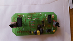
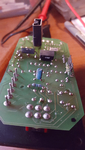
Hi there, I’ve been given a lcd volt / amp meter to repair. See attached photos. The circuit board has burnt the track beyond repair. I have etched a new board and would like some help / advice.
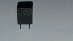
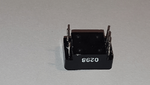
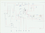
There is a small (8.5mm * 12.5mm) component which I cannot identify. It originally had 6 legs although 1 was removed at time of fitting. The original supplier / manufacturer seems to have sanded the part numbers off!
This unit is fitted on a sailing yacht to monitor battery voltage and current. The current can be measured both when charging and discharging.
The supply voltage is 24v dc nominal and the measured voltage is 24v nominal. The battery charger can output 50a max and the current is sensed via a shunt.
The lcd display is similar to the one in the data sheet, I have powered it with 5 to 12v dc and it seems happy.
From the circuit diagram the supply power feeds a voltage control chip LM317t and outputs 5.2v
The measured voltage is the same as supply and is fed to the IN-lo and IN-hi terminals via relay1 through a voltage divider, one volt displayed = one mv.
When in amps mode the voltage is read direct from the shunt, again one amp = one mv.
What seems odd is the voltage at the lcd supply pins has increased to 9.58 v dc, so I’m guessing the 4093 and BC549 transistors increase voltage then feed it through the signal diodes.
Now it all seems to work OK except the display seems to fluctuate too much with a steady input. Can anyone identify the mystery component? And what is it and what does it do?
Also can anyone tell me what the 4093BE IC does along with the transistors and signal diodes.
I kind of understand the Schmitt triggers but if anyone can explain the flow through it and the transistors that would be great.
It seems very complicated when if the lcd requires 9,58 volts why not increase output from the LM317t?
Is it possible the mystery component is an Opto isolator? The reason I ask is the display vss is isolated from 0v. The 9.58 volts is accross vss and vdd.
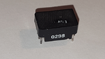
The image of the pcb from solder side is an identical unit fitted and working.
All replies greatly appreciated Roger T.

There is a small (8.5mm * 12.5mm) component which I cannot identify. It originally had 6 legs although 1 was removed at time of fitting. The original supplier / manufacturer seems to have sanded the part numbers off!
This unit is fitted on a sailing yacht to monitor battery voltage and current. The current can be measured both when charging and discharging.
The supply voltage is 24v dc nominal and the measured voltage is 24v nominal. The battery charger can output 50a max and the current is sensed via a shunt.
The lcd display is similar to the one in the data sheet, I have powered it with 5 to 12v dc and it seems happy.
From the circuit diagram the supply power feeds a voltage control chip LM317t and outputs 5.2v
The measured voltage is the same as supply and is fed to the IN-lo and IN-hi terminals via relay1 through a voltage divider, one volt displayed = one mv.
When in amps mode the voltage is read direct from the shunt, again one amp = one mv.
What seems odd is the voltage at the lcd supply pins has increased to 9.58 v dc, so I’m guessing the 4093 and BC549 transistors increase voltage then feed it through the signal diodes.
Now it all seems to work OK except the display seems to fluctuate too much with a steady input. Can anyone identify the mystery component? And what is it and what does it do?
Also can anyone tell me what the 4093BE IC does along with the transistors and signal diodes.
I kind of understand the Schmitt triggers but if anyone can explain the flow through it and the transistors that would be great.
It seems very complicated when if the lcd requires 9,58 volts why not increase output from the LM317t?
Is it possible the mystery component is an Opto isolator? The reason I ask is the display vss is isolated from 0v. The 9.58 volts is accross vss and vdd.
The image of the pcb from solder side is an identical unit fitted and working.
All replies greatly appreciated Roger T.