Puppet123
Full Member level 6
I have a question about IC Layout and Grounding.
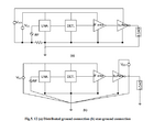
In this IC layout below, I have 4 blocks, all connected to the same ground.
When IC layout is done and chip is fabricated, the way the buffers are grounded (and their IC layout) caused the circuit to oscillate.
In IC layout then would the solution be (b) here or even separating the LNA, having its own ground and the detector and IF having their own shared ground and the buffer, as shown having its own ground plane - and then each having their own ground pads - with all IC ground pads connected to the PCB ground plane.
What do you think ? Any ideas, advice, opinions, please share ?
The detector also contains a mixer.
This is running at 20 +GHz (the LNA is at least).
Thank you.