Piet de Pad
Junior Member level 2
Hi,
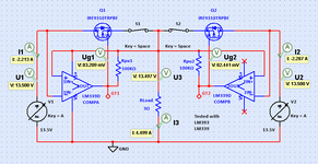
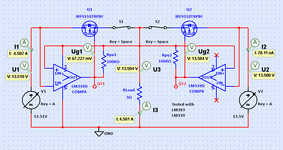
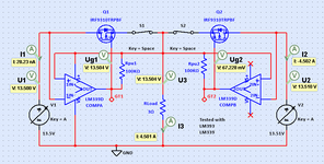
Does anyone have experience with parallel switching of power supplies like I do depicted in the schematics below. I have designed and simulated an ORing or ideal diode based on simple components. It's based on a PMOSFET and a LM393 or LM339 comparator. It works amazingly well as far as my simulations are concerned.
The switching window is 10mV, which is the difference between the two supply voltages to select one of the two power supplies. Within this window both, power supplies work in parallel. Outside the window, only one power supply works. When you remove one of the supplies, the other one takes over.The three figures show the various states the ORing can be in.
Fig 1 shows the ORing when both power supplies have equal voltages. Both power supplies current. In fig 2,3 you can see that with a difference of 10 mV between the two power supplies, one or the other is selected.
Before I build it, I would like to know if there are others who have done this before. let me know in de commends if you have or have suggestion for things I have overlooked.
Thanks
Does anyone have experience with parallel switching of power supplies like I do depicted in the schematics below. I have designed and simulated an ORing or ideal diode based on simple components. It's based on a PMOSFET and a LM393 or LM339 comparator. It works amazingly well as far as my simulations are concerned.
The switching window is 10mV, which is the difference between the two supply voltages to select one of the two power supplies. Within this window both, power supplies work in parallel. Outside the window, only one power supply works. When you remove one of the supplies, the other one takes over.The three figures show the various states the ORing can be in.
Fig 1 shows the ORing when both power supplies have equal voltages. Both power supplies current. In fig 2,3 you can see that with a difference of 10 mV between the two power supplies, one or the other is selected.
Before I build it, I would like to know if there are others who have done this before. let me know in de commends if you have or have suggestion for things I have overlooked.


Thanks