Continue to Site

Welcome to EDAboard.com

Welcome to our site! EDAboard.com is an international Electronics Discussion Forum focused on EDA software, circuits, schematics, books, theory, papers, asic, pld, 8051, DSP, Network, RF, Analog Design, PCB, Service Manuals... and a whole lot more! To participate you need to register. Registration is free. Click here to register now.

Divide by 2 Counter using only logic gates - Verilog

Status
Not open for further replies.

rohith94

Newbie level 3
Joined
Feb 1, 2017
Messages
3
Helped
0
Reputation
0
Reaction score
0
Trophy points
1
Activity points
22
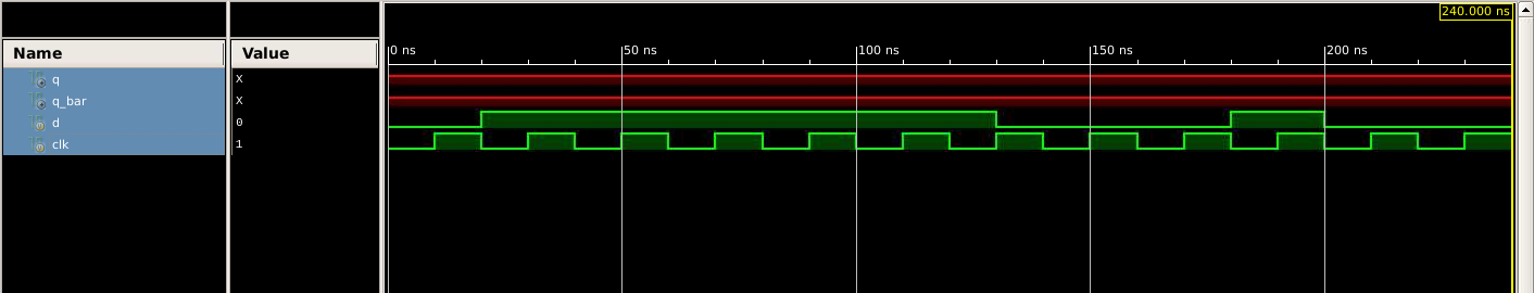
I designed a D-Flip Flop using only logic gates (i.e., gate level design) - Verilog. Now I want to convert this into a divide by 2 counter. Can anyone help me with this?

My Code:

Code Verilog - [expand]
1
2
3
4
5
6
7
8
9
10
11
12
13
14
15
16
17
18
19
20
21
22
23
24
25
26
27
28
29
30
`timescale 1ns / 1ps
module d_ff_gates(d,clk,q,q_bar);
input clk;
input d;
output q, q_bar;
 
wire n1,n2,n3,q_bar_n,clk1;
wire cn,dn,n4,n5,n6;
 
// First Latch
not (n1,d);
not (clk1,clk);
nand (n2,d,clk1);
nand (n3,n1,clk1);
 
nand (dn,q_bar_n,n2);
nand (q_bar_n,dn,n3);
 
// Second Latch
not (cn,clk1);
 
not (n4,dn);
 
nand (n5,dn,cn);
nand (n6,n4,cn);
 
nand (q,q_bar,n5);
nand (q_bar,q,n6);
 
endmodule

 
Last edited by a moderator:

Hi,

Something like this: D = not Q

Klaus
 

So, I added the following line to the code
Code:
not(d,q)

with the test bench being
Code:
`timescale 1ns / 1ps
module d_ff_gates_tb();

reg d;
reg clk;

wire q;
wire q_bar;

initial
begin
d = 0;
clk = 0;
end

always begin
#10 clk = ~clk;
//#10 d = clk;
end

d_ff_gates U0(
d,
clk,
q,
q_bar
);

The verilog code still doesnt work.
 

Did you verify DFF operation with a test bench?

The verilog code still doesnt work.
Means more specifically what?

Surely you can't drive d by an inverter inside the DFF module and still have d as an input port, as the test bench suggests.
 

This is how my output waveform looks like.


Uh, the original d_ff code works fine if you write your testbench correctly.
Capture.PNG


Code Verilog - [expand]
1
2
3
4
5
6
initial begin
    d = 0;
  end
  always @* begin
    d = ~q;
  end


This code is needed if you want the d_ff input to be the inverted version of q (i.e. a divide by 2).

- - - Updated - - -

Or even easier is to compile with sv so you can use the bit type which can only be 0 or 1 so no Xs or Us will not be produced by your testbench, then the code can be as simple as:

Code Verilog - [expand]
1
2
3
4
5
6
7
8
9
10
11
12
13
14
15
reg clk = 0;
 
  bit q;
  bit q_bar;
 
  always begin
    #10 clk = ~clk;
  end
 
  d_ff_gates U0(
    .d      (q_bar),
    .clk    (clk),
    .q      (q),
    .q_bar  (q_bar)
  );


Waveform using bit:
Capture.PNG
 
Are you talking "structural verilog" where everything
uses (say) nand2, nand3, inv constructs?

If so, be aware that this scheme will not work with
delay-less gates; NAND and TINV latches depend
on "short term memory" (from gate delays) in the
switching action, and with zero delay can fail to
"make up their mind" about coincident, conflicting
logic-value transitions.
 

Status
Not open for further replies.

Part and Inventory Search

Welcome to EDABoard.com

Sponsor

Back
Top