Continue to Site

Welcome to EDAboard.com

Welcome to our site! EDAboard.com is an international Electronics Discussion Forum focused on EDA software, circuits, schematics, books, theory, papers, asic, pld, 8051, DSP, Network, RF, Analog Design, PCB, Service Manuals... and a whole lot more! To participate you need to register. Registration is free. Click here to register now.

Design of a classical 1 stage op-amp

Status
Not open for further replies.

tisheebird

Member level 5
Joined
Feb 23, 2017
Messages
88
Helped
0
Reputation
0
Reaction score
0
Trophy points
6
Activity points
662
Hello,

I have designed a 1 stage op-amp with the bias current of 2uA. ICMR- is 0.7V and ICMR+ is 1.62V. I want to check the output impedance and gain of my op-amp. so could you please suggest what should be the input value so that i can see the output resistance and gain of the system.?

Please guide me with the solution
 

So you are asking us to tell us how to find some circuit parameters for a circuit we do not know?
 
... could you please suggest what should be the input value so that i can see the output resistance and gain of the system.?

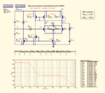
Pls. find here an example for gain vs. frequency - and output range: 1-stage-OTA_output-range_and_gain.png

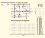
For output impedance vs. frequency remove the input voltage source (or set it to zero), remove the transient simulation, and connect a dc-capacitor-blocked ac unit (1A) current source to the output. Then run an ac simulation and plot Vout vs. frequency. The shown Vout voltage corresponds directly to the (short-circuit) output impedance (1e6 ≙ MV ≙ MΩ , because of the division by i=1A) :
1-stage-OTA_output-impedance.png
 

Hello,
Thanks :) Erikl, Were are these pictures/simulation coming from ?
regards
 

Thanks a lot...But I have designed 1 stage op-amp. I am telling you the W/L of each transistor. Could you please check if the amplifier is performing okay.
Actually in my whole system I have used this amplifier and the output of the system is coming good. But I really would like to know if the amplifier is good or not.

So (W/L)3= (W/L)4 = 0.5u/2u, Input transistors (NMOS)(W/L)1=(W/L)2= 2u/0.5u. Current source (W/L)o= 0.5u/2u. The bias current is 2uA.

View attachment op-amp.pdf

- - - Updated - - -

From simulations with my schematic, with the free Qucs from sourceforge.


Please check for this circuit. In my previous message I have given you the sizes. Please check everything like DC, AC. Please could you confirm me if it is working as an amplifier.View attachment op-amp.pdf

180 nm CMOS process with supply of 1.8V..
 

Please check for this circuit.

Not possible - I don't have your models. I just wanted to show you how you can simulate the gain and the output impedance.

Now it's your job!
 

Not possible - I don't have your models. I just wanted to show you how you can simulate the gain and the output impedance.

Now it's your job!


Thank you. But when I give same inputs on both the inputs then I am have a nice AC plot and DC values. But the question is when I varry the input such as +ve input is 1.6V and -ve input is 1V then the DC points varry and transistors are not in saturation region. So am I doing it right by this.?
 

But the question is when I varry the input such as +ve input is 1.6V and -ve input is 1V then the DC points varry and transistors are not in saturation region.
Why would you do this? To gain and output impedance are small signal parameters determined in AC analysis with useful amplifier bias. For higher gain amplifiers, an auxiliary feedback network is the usual way to set the bias point. Surely the input difference voltage will be near to zero.
 

Why would you do this? To gain and output impedance are small signal parameters determined in AC analysis with useful amplifier bias. For higher gain amplifiers, an auxiliary feedback network is the usual way to set the bias point. Surely the input difference voltage will be near to zero.

Yes you are right. Here is my case. Please guide me what is the right way..IMG_20180401_123213725_HDR.jpg

When I do DC simulation, the =+ve DC voltage is 1.62V and if my Vref is 1.62V then the amplifier is working. But if my Vref is suppose 1V then amplifier is not functional.
So that means in the beginning, i have to set Vref=1.62V..??
 

Not sure about the actual amplifier topology. "Classical single stage OP" in my view refers to a differential pair with some combination of current mirrors and a single ended output. Suitable bias feedback network depends on output voltage range and input common mode range. Preferably the bias point is set somewhere in the middle of it.
 

Not sure about the actual amplifier topology. "Classical single stage OP" in my view refers to a differential pair with some combination of current mirrors and a single ended output. Suitable bias feedback network depends on output voltage range and input common mode range. Preferably the bias point is set somewhere in the middle of it.

yes you are right. thanks...also I would like to know if a system is a 1 pole system then do you need to check the relative stability or it is always stable.?
 

Status
Not open for further replies.

Part and Inventory Search

Welcome to EDABoard.com

Sponsor

Back
Top