Continue to Site

Welcome to EDAboard.com

Welcome to our site! EDAboard.com is an international Electronics Discussion Forum focused on EDA software, circuits, schematics, books, theory, papers, asic, pld, 8051, DSP, Network, RF, Analog Design, PCB, Service Manuals... and a whole lot more! To participate you need to register. Registration is free. Click here to register now.

Demultiplexer

Mancoba

Newbie
Joined
Nov 28, 2023
Messages
2
Helped
0
Reputation
0
Reaction score
0
Trophy points
1
Activity points
19
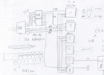
Hello everyone, I'm new here and currently working on a digital circuit design. I'm having trouble figuring out a concept for assembling 8x 1 to 8 demultiplexers in a way that consumes minimal digital outputs. I have an NI-DAQ card with 16 digital IO, and I want to use as few digital outputs from my DAQ card as possible—ideally just around 8 bits to control the demultiplexers. How can I solve this problem? Has anyone built something similar and has a sample circuit ready for me? English isn't my native language either.
 
Hi,

please draw a sketch.

There is so much unclear. Like:
* DAQ .. usually means analog data acquisition. So "analog input", but you talk about "digital output". Maybe you have a special DAQ module in mind, then give a link to it´s datasheet.
* what does 8x 1 to 8 DEMUX mean? All DEMUX are controlled in parallel or individually?

And yes, all about digital levels, speed, available interfaces...
maybe also the analog side requirements: cross talk, ON resitance, OFF attenuation ...

Klaus
 
thanks for your reply and support. i have found a solution. I am just a beginner in digital circuit design... I have it on a sheet of paper. it looks a bit messy, but I hope you can understand my sketch. A two Part address of 3Bits + 3 Bits (CS) = 6 Bits in Total.
 

Attachments

  • Pic.PNG
    Pic.PNG
    620 KB · Views: 59
Hi,

this currently is a 1 to 64 DEMUX using 9 ICs.

You could also use 5 pcs 1:16 DEMUX ICs.

***
But still the drawing is unclear.
It says DAC. A DAC is a digital-to-analog-converter. Digital input, analog output. But your sketch shows 8 outputs used as digital signals.

Klaus
 
This is a SOC one chip solution. Note it uses most of GPIO so not knowing
your total design/schematic it could be revised to a family with more GPIO.

PSOC 5LP, depending on origin DAC 's data input. and other details. Possibly
PSOC 6 to get more GPIO for other functions.

Almost a codeless design you would need 1 start instruction for DAC.

Details such as speed, complete schematic of course need review.

1701209956515.png


Regards, Dana.
--- Updated ---

Note there is a lot of other stuff on this part, that you can use or ignore.

1701212657814.png


Multiple copies of many of these resiources. And for the adventuress one can
design your own resopuce using schematic capture of above and / or Verilog.

Compiler and IDE, PSOC Creator, free.


Regards, Dana.
 
Last edited:

LaTeX Commands Quick-Menu:

Part and Inventory Search

Welcome to EDABoard.com

Sponsor

Back
Top