Continue to Site

Welcome to EDAboard.com

Welcome to our site! EDAboard.com is an international Electronics Discussion Forum focused on EDA software, circuits, schematics, books, theory, papers, asic, pld, 8051, DSP, Network, RF, Analog Design, PCB, Service Manuals... and a whole lot more! To participate you need to register. Registration is free. Click here to register now.

Constant current LED Driver Circuit

gauravkothari23

Advanced Member level 2
Joined
Mar 21, 2015
Messages
640
Helped
5
Reputation
10
Reaction score
4
Trophy points
1,298
Activity points
6,922
Hi All.
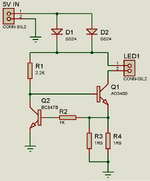
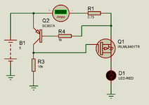
I Am using a Constant current circuit (Attached) to drive the SMD LED's.
i am using Approx 750mA of Current to drive a LED's with 5V input which is working fine. Mosfet used is SMD SOT23 Package AO3400. My problem is the mosfet gets extremely hot around 70 to 75 degree Celsius within 10 to 12 seconds.
Can anybody please suggest me why the mosfet is getting hot and how can i avoid it. What changes are required to be done in my existing circuit.
 

Attachments

  • CC Circuit.png
    CC Circuit.png
    20.2 KB · Views: 148
KlausST. can you please let me know why the voltage across the mosfet is 1.12V and not 0.25 as per the datasheet.
How did you make it that the volt across Mosfet would be 1V
It is a linear regulator, so Ohm's Law prevails. 5V* 0.75A= 15/4 W =3.75 So Power will be dissipated according to the shared current *V.

If you had a lower Vcc supply then you will have a lower drop.

Always choose twice the power rating than will be used.
If you want the temp rise to be 50% of the 125'C rated temperature and increase R to drop Vds=0.25V and the remainder shared by Vf & Rs
--- Updated ---

This is another poor linear design because it does not sense current or thermal effects but it has an LED with Vf just slightly less than the supply.

1708297083932.png


You can sense with a very small R value then amplify it and regulate current.
1708297263547.png


But realistically there are far better designs in IC's for LED drivers so these become learning aids to how not to design a high power LED driver.
--- Updated ---


This is one way to salvage your design is to raise the reference voltage for Vb by raising Ve with Ie*Re.

1708298519827.png

You can lower Vds even more , but is not necessary. But if you had to say you had a std FET with Vt=3V then you can still use an NFET move the current sense to the high side. Moving the source to ground thus raises Vgs/Vgs(th) ratio which lowers RdsOn but now you lose your NPN Vbe reference.

Moving the current sense to the high side now inverts your logic. Now a lower voltage indicates rising current, so the current-limit for the gate cutoff driver would have to change.
 

Attachments

  • 1708298378403.png
    1708298378403.png
    71.4 KB · Views: 42
Last edited:
It is a linear regulator, so Ohm's Law prevails. 5V* 0.75A= 15/4 W =3.75 So Power will be dissipated according to the shared current *V.

If you had a lower Vcc supply then you will have a lower drop.

Always choose twice the power rating than will be used.
If you want the temp rise to be 50% of the 125'C rated temperature and increase R to drop Vds=0.25V and the remainder shared by Vf & Rs
--- Updated ---

This is another poor linear design because it does not sense current or thermal effects but it has an LED with Vf just slightly less than the supply.

View attachment 188802

You can sense with a very small R value then amplify it and regulate current.
View attachment 188803

But realistically there are far better designs in IC's for LED drivers so these become learning aids to how not to design a high power LED driver.
--- Updated ---


This is one way to salvage your design is to raise the reference voltage for Vb by raising Ve with Ie*Re.

View attachment 188805
You can lower Vds even more , but is not necessary. But if you had to say you had a std FET with Vt=3V then you can still use an NFET move the current sense to the high side. Moving the source to ground thus raises Vgs/Vgs(th) ratio which lowers RdsOn but now you lose your NPN Vbe reference.

Moving the current sense to the high side now inverts your logic. Now a lower voltage indicates rising current, so the current-limit for the gate cutoff driver would have to change.
For high side current sensing, i have to use P Channel mosfet...??
and even i have tried circuit you sent with alteration. add 1.5K resistor to Transistor E and GND. but the problem is the same. Voltage across the mosfet is 1V
 
KlausST. can you please let me know why the voltage across the mosfet is 1.12V and not 0.25 as per the datasheet.
How did you make it that the volt across Mosfet would be 1V
Not 0.25V but 0.025V !!!

You have an input voltage of 5V.
So the total voltage across each part in series needs to be 5V. (There is no way around this, in every circuit)

Diodes: lets say 0.35V
LEDS: 2.9V
Transisitor: rest
Resistors: 0.6V

Transistor: 5V - ( 0.35V + 2.9V + 0.6V) = 5V - 3.85V = 1.15V.

Your circuit is designed for the transistor to regulate. Regulate = adjusting the voltage ... in a way that above equation is true.

Klaus
Excatly Got you point.
Will try High side Current sensing as you suggested.
But for high side current sensing
do i have to use P channel mosfet and PNP transistor as per the circuit attached.
 

Attachments

  • P Channel Current.png
    P Channel Current.png
    19.2 KB · Views: 30
Hi,

I´m not sure you understood.

* I did not suggest high side sensing
* I said this (sum of all voltages = 5V) is true for every circuit, thus also for high side sensing

So high side sensing will not reduce overall power dissipation. You gain nothing in this regard.

Klaus
 
Hi,

I´m not sure you understood.

* I did not suggest high side sensing
* I said this (sum of all voltages = 5V) is true for every circuit, thus also for high side sensing

So high side sensing will not reduce overall power dissipation. You gain nothing in this regard.

Klaus
ok, so whatever circuit i use, have to face the heating problem as well.
 
Hi,

why do we need to repeat?

from post #5:
So to reduce the dissipated heat you only have these options:
* reduce V_in
* increase V_Led (maybe by using two or more in series)
* reduce the LED current
* .... or use switch mode circuit instead of linear circuit

Klaus
 
Are you using a breadboard with no heatsink?

What Led Vf @ 750mA? post link of datasheet.
What is your skill level? age? training? so I know what to suggest.
For high side current sensing, i have to use P Channel mosfet...??
and even i have tried circuit you sent with alteration. add 1.5K resistor to Transistor E and GND. but the problem is the same. Voltage across the mosfet is 1V
Show layout in photo and exact parts list for each with values for R1,R2,R3 for ohms and R3 must be rated for >= 2W along with datasheet for FET and LED.

I posted a solution where it will not overheat based on your comments.
1708349785758.png

LED also needs a big heatsink just like everything else. You cannot expect your design to use almost 4 Watts in a tight little package and not burn up.

Can you post a photo of your design too?


If you are using AO3400 (open link) measure Vgs. It must be > 2.5V, if not find out why. Using my R1,R2,R3 above with 2 Ohms 2 W or Thevenin equivalent ( do you understand this term?) Look at my voltages and see which of yours is not similar. The resistors are rated for max power at 150'C or a 125'C rise so using 1.236W rated for 2W means 1.236/2W*100% it will rise to about 100'C but the FET shows above 120mV / 786 mA = 152 mOhm so my approximation was a bit high for this but Pd = .12V*.79A = 0.12W and this tiny FET must use a heatsink.
1708350124883.png


ON datasheet.
1708350784741.png

See the superscript letters A D. especially A With 2oz Copper this acts as a heatsink, without this it it can be as much as 200'C/W. So my calculation is 0.12W * 200'C/W with 120 mV drop @ 786mA means it will only rise 24'C above 25'C ambient, which assumes you are not self-heating your cramped case even hotter, which may be untrue.
in open ambient free-air circulating your FET should be 50'C max which is still hot to touch but safe for reliable operation. If none of this makes sense, search for thermal design and read on this site or others. But please respond as I requested above.

1708350833136.png
 
Hi,

all the recently posted schematics will generate the same overall heat (power dissipation) as the circuit of post#1.

Circuit of post#29 shifts the power dissipation from transitor to resistor. But it does not cause less overall heat. Only you will know if this is a benefit or not.
The problem with this circuit is that it just lowers the headroom for a true "constant current" (headline) source to operate. A 5V power supply is never perfect 5V.
A standard 7805 for example has an initial tolerance of +/-4% (TI).. while the given circuit can only regulate -2%. But you additionally have voltage drops because wire resitances, part tolerances, temperature drifts ...
So if the true available LED supply voltage drops by just 2% (referred to 5.0V) .. there is no regulation anymore ... the circuit then is nothing better than a simple resistor.
It loses the "constant current" feature.

Klaus
 

LaTeX Commands Quick-Menu:

Part and Inventory Search

Welcome to EDABoard.com

Sponsor

Back
Top