Continue to Site

Welcome to EDAboard.com

Welcome to our site! EDAboard.com is an international Electronics Discussion Forum focused on EDA software, circuits, schematics, books, theory, papers, asic, pld, 8051, DSP, Network, RF, Analog Design, PCB, Service Manuals... and a whole lot more! To participate you need to register. Registration is free. Click here to register now.

communicating EFR32FG14 with MCP3421

Status
Not open for further replies.

yefj

Advanced Member level 4
Joined
Sep 12, 2019
Messages
1,236
Helped
1
Reputation
2
Reaction score
3
Trophy points
38
Activity points
7,432
Hello,I am try to communicate with MCP3421 over I2C,from the data sheet table shown bellow the configuration register should be X0011100.

G1,G0=00=X1 Gain
S1,S0=11=18 bits
O*/C=1 continues mode
C1,C0=00=dont care
bit7 RDY*-X-Not in our control

In section 5.3.1 they describe the I2C procedure for the first part:
St->1101,000,0(device code,defalt factory adrress,write bit)->
then We send configuration byte(for config register):
X0011100

I dont know what value to put in the RDY* bit?

So till now the structure is St->ADDRESS+write(0)->ACK->Configuration Byte->ACK->Stop by master

The big issue is with the second part of reading converter data:
I send St->ADDRESS+read(1) and i should get ACK->4bytes(3 data,1 config bytes)->NACK->Stop
I cand understand this part of the data sheet:

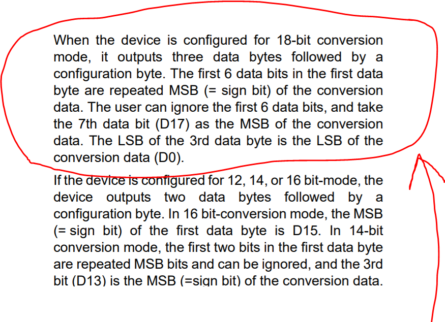
We suppose to get 3 data bite and configuration byte,
from the diagram in page 20 i cant see what are D17,D16 are for?
if we ignore 6 bits then we dont have animore 18 bit resolution?
And i could not see how to controlif i want to add configuration bit?
I'll be glad to have some itnuition regarding these points.
Thanks.


1608644285155.png

1608638967166.png
 

I dont know what value to put in the RDY* bit?
Datasheet section 5.1.1 and 5.1.2 tells what to do.

bit7 RDY*-X-Not in our control
Not true. You see it is marked READ and WRITE. Not READ only. So you may use it, especially in ONE-SHOT CONVERSION MODE


We suppose to get 3 data bite and configuration byte,
from the diagram in page 20 i cant see what are D17,D16 are for?
if we ignore 6 bits then we dont have animore 18 bit resolution?
And i could not see how to controlif i want to add configuration bit?
I'll be glad to have some itnuition regarding these points.
What is unclear?
* each byte consists of 8 bits.; lets mark each bit with a "B" --> 1 byte = BBBBBBBB
* the first byte: the text says you may ignore the first 6 bits: lets mark the "ignore" bits as "X" --> XXXXXXBB

so the three databytes are: XXXXXXBB BBBBBBBB BBBBBBBB

I see 18 bits "B" --> 18 bits resolution.
D17 down to D0 are 18 data bits

***
in the end the description is clear .. and the timng diagram is clear ... for me.
But it seems not to be clear for you. So please tell what is unclear. We can´t know your doubts unless you write them here.

Klaus
 

Hello Klauss,
regarding single shot mode 5.1.2:
When the convertion is over RDY*=0 , and when it recieves another command then RDY goes 1ץ
So it act as a flag and we need to write RDY*=1 in order to make another conversion


Regarding Continues mode 5.1.1:
RDY* turns 0 when convertion is completed
RDY* is 1 when we read the data
So what is the RDY* value when convertion is in progress?
And what do i write in config RDY* when we want to work in continues mode?

Regarding the reading of the 18 bits:
So by your explanation the MSB B (B on the most left) is the sign bit?
so 18th bit is sign and the rest 17 bits is data.
Is it complement 2 representation?
Thanks
 

Hi,

And what do i write in config RDY* when we want to work in continues mode?
And this is what the datasheet says:
Writing RDY bit with the write command:
Continuous Conversion mode: No effect


Is it complement 2 representation?
And this is what the datasheet says:
4.9.1 DIGITAL OUTPUT CODE FROM
DEVICE
The digital output code is proportional to the input
voltage and PGA settings. The output data format is a
binary two’s complement.


It seems you need one to read the datasheet for you.

When you want to know whether the output is in 2s complement representation:
Try to use the PDF reader's search function: for example "complement"
It's much faster than writing a post.

Klaus
 
  • Like
Reactions: yefj

    yefj

    Points: 2
    Helpful Answer Positive Rating
hello
am wonder why you don't search for a header file (h.file )or (c.file) and include it with your source code .MCP3421 beyond to Microchip and if it includes some differences lib.function . you may could do some modifications for it . it is a simple way than you make up(design) your own (h.file). there is application in Arduino pages


kamal.
 

Hello Klauss,sorry i didnt see that spot .i wiil try to read more carefully.
 

Hello, We need to connect I2C SDA SCL from expansion header to mcp3421 ADC on a bread board.
based on the efr32fg14 starter kit i haved connected pin20 3v3,pin16 I2C_SDA,pin15 I2C_SCL,pin1 GND

Based on the diagram bellow,We have the expansion header and the Si7021 connected on the same LOCATION
So i think that in order for us to dissable the SI7021 sensor and make the expansion header connected to mcp3421
we need to disable PD15 in the code.

then i have shown bellow a photo from paper ,How the I2C communication should look like the calculation of device address D0 and calculation of config byte 1C.

Then i have made a voltage divider to input single ended my mcp3421 in scope photo 1A where we se the input is 2.4V and pk-pk 194mv.

Then as shown in photos 2A to 2D I have connected the I2C 3.3,gnd,extension header pins to their corresponding MCP.Also i have connected 5.1Kohm resistors to SDA and SCL to 3.3v to make the signal better.
I have used I2C_FLAG_WRITE_READ flag which has the structure shown bellow.
In the code i have set to recieve 4 bits (3 data and 1 config as in the data sheet of mcp3421 bellow).
the full code is shown in the end
unfortunetly i am allowed to upload only 10 photos per comment so i add the I2C scope photos bellow in the next comment
The I2C diagram that was recieved shown in the last photos bellow ,we see a cyclic structure where write at the start the slave sends NACK to my 0xD0 (adress+w)
from mcp3421 Data sheet page 18 device code is 1101 and A2-A0 is 000 plus write bit (0) so the total is 11010000 which is 0xD0
Why its no accepting this data?
Thanks.


EFR32FG14 starter kit:
EFR32FG14 data sheet:
EFR32FG14 I2C API
Mcp 3421 datasheet:

1608728463656.png

1608729402681.png

1608729520798.png


1608730934810.png

1608731137558.png

1608731521994.png

1608731558785.png

1608731623085.png

1608731666777.png


1608732491522.png


Code:
#include "em_usart.h"
#include "em_ldma.h"

/////////////////
#include "stddef.h"
#include "em_system.h"
#include "em_device.h"
#include "em_chip.h"
#include "em_cmu.h"
#include "em_emu.h"
#include "em_gpio.h"
#include "i2cspm.h"
#include "si7013.h"
#include "sl_sleeptimer.h"
#include "graphics.h"
#include "em_adc.h"
#include "bspconfig.h"


uint8_t com1[1] = {0x1C}; //config command

//page 20 of data sheet
uint8_t i2c_rxBuffer[4]; //[0]-2nd Byte [1]-3rd byte [2]-4th byte [3]-5th config byte
void initUSART1 (void)
{
    CMU_ClockEnable(cmuClock_GPIO, true);
    CMU_ClockEnable(cmuClock_USART1, true);

    // Configure GPIO mode
    GPIO_PinModeSet(gpioPortC, 8, gpioModePushPull, 0); // US1_CLK is push pull
    GPIO_PinModeSet(gpioPortC, 9, gpioModePushPull, 1); // US1_CS is push pull
    GPIO_PinModeSet(gpioPortC, 6, gpioModePushPull, 1); // US1_TX (MOSI) is push pull
    GPIO_PinModeSet(gpioPortC, 7, gpioModeInput, 1);    // US1_RX (MISO) is input
    GPIO_PinModeSet(gpioPortF, 7, gpioModeInput, 1);    // delay gpio

    // Start with default config, then modify as necessary
    USART_InitSync_TypeDef config = USART_INITSYNC_DEFAULT;
    config.master       = true;            // master mode
    config.baudrate     = 1000000;         // CLK freq is 1 MHz
    config.autoCsEnable = true;            // CS pin controlled by hardware, not firmware
    config.clockMode    = usartClockMode0; // clock idle low, sample on rising/first edge
    config.autoCsEnable = true;            // CS pin controlled by  firmware
    config.msbf         = true;            // send MSB first
    config.enable       = usartDisable;    // Make sure to keep USART disabled until it's all set up
    USART_InitSync(USART1, &config);

    // Set USART pin locations
    USART1->ROUTELOC0 = (USART_ROUTELOC0_CLKLOC_LOC11) | // US1_CLK       on location 11 = PC8 per datasheet section 6.4 = EXP Header pin 8
                        (USART_ROUTELOC0_CSLOC_LOC11)  | // US1_CS        on location 11 = PC9 per datasheet section 6.4 = EXP Header pin 10
                        (USART_ROUTELOC0_TXLOC_LOC11)  | // US1_TX (MOSI) on location 11 = PC6 per datasheet section 6.4 = EXP Header pin 4
                        (USART_ROUTELOC0_RXLOC_LOC11);   // US1_RX (MISO) on location 11 = PC7 per datasheet section 6.4 = EXP Header pin 6

    // Enable USART pins
    USART1->ROUTEPEN = USART_ROUTEPEN_CLKPEN | USART_ROUTEPEN_CSPEN | USART_ROUTEPEN_TXPEN | USART_ROUTEPEN_RXPEN;


    // Enable USART1
    USART_Enable(USART1, usartEnable);
    ////////////////////////////////////////////
    //UART INITLIZATION

    USART_InitAsync_TypeDef init = USART_INITASYNC_DEFAULT;


     // Enable oscillator to GPIO and USART0 modules

     CMU_ClockEnable(cmuClock_USART0, true);

     // set pin modes for UART TX and RX pins
     GPIO_PinModeSet(gpioPortA, 1, gpioModeInput, 0);
     GPIO_PinModeSet(gpioPortA, 0, gpioModePushPull, 1);

     // Initialize USART asynchronous mode and route pins
     USART_InitAsync(USART0, &init);
     USART0->ROUTELOC0 = USART_ROUTELOC0_RXLOC_LOC0 | USART_ROUTELOC0_TXLOC_LOC0;
     USART0->ROUTEPEN |= USART_ROUTEPEN_TXPEN | USART_ROUTEPEN_RXPEN;

}//end usart init

int main(void)

{

I2C_TransferSeq_TypeDef i2cTransfer;

I2C_TransferReturn_TypeDef result;


I2CSPM_Init_TypeDef i2cInit = I2CSPM_INIT_DEFAULT;


/* Chip errata */

CHIP_Init();
initUSART1();


// Enabling clock to the I2C, GPIO, LE

CMU_ClockEnable(cmuClock_I2C0, true);

CMU_ClockEnable(cmuClock_GPIO, true);

CMU_ClockEnable(cmuClock_HFLE, true);


// Starting LFXO and waiting until it is stable

CMU_OscillatorEnable(cmuOsc_LFXO, true, true);


I2CSPM_Init(&i2cInit);

// In order to enable the I2C0_SCL function in PC10 you need to use ROUTE 14

// In order to enable the I2C0_SDA function in PC11 you need to use ROUTE 16

//Also note that there's a GPIO pin PD15 that need to be set to high in order to route the signals to the sensor,

// Using PC10 (SCL) and PC11 (SDA)

  GPIO_PinModeSet(gpioPortC, 10, gpioModeWiredAndPullUp, 1);

  GPIO_PinModeSet(gpioPortC, 11, gpioModeWiredAndPullUp, 1);


// GPIO_PinModeSet(gpioPortC, 10, gpioModeWiredAnd, 1);

//  GPIO_PinModeSet(gpioPortC, 11, gpioModeWiredAnd, 1);

  //Si7021 switch off

  GPIO_PinModeSet(gpioPortD, 15, gpioModePushPull, 0);


  // Enable pins at location 15 as specified in datasheet

  I2C0->ROUTEPEN = I2C_ROUTEPEN_SDAPEN | I2C_ROUTEPEN_SCLPEN;

  I2C0->ROUTELOC0 = (I2C0->ROUTELOC0 & (~_I2C_ROUTELOC0_SDALOC_MASK)) | I2C_ROUTELOC0_SDALOC_LOC16;

  I2C0->ROUTELOC0 = (I2C0->ROUTELOC0 & (~_I2C_ROUTELOC0_SCLLOC_MASK)) | I2C_ROUTELOC0_SCLLOC_LOC14;

  i2cTransfer.flags=I2C_FLAG_WRITE_READ;

  i2cTransfer.addr=0xD0;//address with write

  i2cTransfer.buf[0].data=&com1[0];  // Config byte

  i2cTransfer.buf[0].len=1;    //number bytes in config bytes


  i2cTransfer.buf[1].data=i2c_rxBuffer;

  i2cTransfer.buf[1].len=4;    //4 bytes =3 data and 1 config byte

while(1)

{

  result=I2C_TransferInit(I2C0,&i2cTransfer);


  // Sending data

   while (result == i2cTransferInProgress)

   {

    result = I2C_Transfer(I2C0);

   }

   //When sending data ends
   //SPI sending data
   USART_SpiTransfer(USART1,i2c_rxBuffer[0]);
   USART_SpiTransfer(USART1,i2c_rxBuffer[1]);
   USART_SpiTransfer(USART1,i2c_rxBuffer[2]);

   //send UART
   USART_Tx(USART0, '\n');
      USART_Tx(USART0, i2c_rxBuffer[0]);
      USART_Tx(USART0, i2c_rxBuffer[1]);
      USART_Tx(USART0, i2c_rxBuffer[2]);
      USART_Tx(USART0, 'a');
      USART_Tx(USART0, '\n');


}


}
--- Updated ---

I2C scope photos for my comment:
1608733916833.png

1608733937899.png
 
Last edited:

I have tried to use adress 0x68 instead of 0xD0 as shown bellow,still It gives me NACK.
I am starting to believe that either the MCP is broken
Or the breadboard is not suitable for handling
any suggestions how to debug this situation to find out why i get NACK from the device after adress being sent?
Thanks.

1608841503487.png
 

Status
Not open for further replies.

Part and Inventory Search

Welcome to EDABoard.com

Sponsor

Back
Top