Continue to Site

Welcome to EDAboard.com

Welcome to our site! EDAboard.com is an international Electronics Discussion Forum focused on EDA software, circuits, schematics, books, theory, papers, asic, pld, 8051, DSP, Network, RF, Analog Design, PCB, Service Manuals... and a whole lot more! To participate you need to register. Registration is free. Click here to register now.

Class AB Output Stage with Translinear Loops

Status
Not open for further replies.

wes_s01

Newbie
Joined
Aug 29, 2019
Messages
4
Helped
0
Reputation
0
Reaction score
0
Trophy points
1
Activity points
44
Hello,

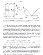
I have been reading the book "Operational Amplifiers" by Johan Huijsing. A mosfet-based class AB output stage is described that has two translinear loops which keep each device at a minimum current when a large current occurs in the other.

Some equations are given, 5.3.7 and I am trying to derive them but am having difficulty getting the same solution.

I am beginning with one equation for each translinear loop and one for each feedback device:

Vgs1 + Vgs4 = Vgs7 + Vgs8
Vgs2 + Vgs3 = Vgs5 + Vgs6
I3 + I4 = 2IB

Am I going in the wrong direction here? Curious if anyone has gone through this algebra before and could lend a hand.

Thanks!
 

Attachments

  • output_stage.PNG
    output_stage.PNG
    128.2 KB · Views: 561

which keep each device at a minimum current when a large current occurs in the other.

The graph illustrates that only one of the output transistors needs to turn on, either M1 or M2.

It needs to turn on at an amount that provides the correct output voltage to the load... no matter what is the load resistance or what voltage the other end sees. (The op amp is designed so the output tries to adopt a voltage that drives the inputs so the inputs are equal voltage to each other.)

We do not want both M1 & M2 to be on simultaneously. That's undesired shoot-through.

On the other hand what about the middle area of the graph? Do we want the output to go high impedance? I suppose we do not. It's a question of balancing two goals:

(a) what is electrically valid, versus (b) what is practical.

The device can't create middle volt levels directly, so we resort to a workaround, namely to provide finite resistance to supply positive and finite resistance to supply negative (simply, a voltage divider). It's not exactly shoot-through yet we allow a minimal current flow so that the load has access to a midway volt level.

So the circuit (or I guess the trans-linear loops) are designed so that the N-device turn-On threshold slightly overlaps the P-device turn-On threshold.
 

Sorry I don't know how to post formula in text...

If you simulate the circuit, you will see that Iq maybe not exactly equal to what derived here, Iq is influenced by Vdd hardly, hence the output driving capaciblity varies among large Vsupply range. The reason is that Vds maybe not equal for all transistors in translinear loop.

Anyway this usually doesn't matter if there is no strict requirements on idle current or you have a fixed Vsupply. The point is that we want both M1 and M2 are slightly on, as BradtheRad said.
translinear.jpg
 
Last edited:

Status
Not open for further replies.

Part and Inventory Search

Welcome to EDABoard.com

Sponsor

Back
Top