Continue to Site

Welcome to EDAboard.com

Welcome to our site! EDAboard.com is an international Electronics Discussion Forum focused on EDA software, circuits, schematics, books, theory, papers, asic, pld, 8051, DSP, Network, RF, Analog Design, PCB, Service Manuals... and a whole lot more! To participate you need to register. Registration is free. Click here to register now.

Class AB, B Circuit Design

Status
Not open for further replies.

michaelScott

Junior Member level 2
Joined
Mar 19, 2022
Messages
24
Helped
0
Reputation
0
Reaction score
0
Trophy points
1
Activity points
161
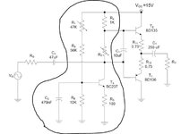
Hello everyone, I'm having difficulty to understand the circuit below. Could you please help me about that.
What C1 transistor stands for? and What the rectangled area's purpose for the circuit.
How is it able to change the class ab and b configuration just by changing the R1 and R2 resistor values.
Thanks in advance.
 

Attachments

  • qweqw.JPG
    qweqw.JPG
    41.9 KB · Views: 152

Role of the circled section:

1) amplify voltage of the incoming signal
2) shift its DC level to a proper operating point
3) Use it to bias the final output transistors

The variable resistors adjust DC level (and perhaps gain as well), to achieve balanced response in the positive and negative waveforms.
 
R2 sets the idle ( quiescent ) current in the output pair of transistors

R1 also affects this by altering the current thru R2, and hence its volt drop

in general it is not a good circuit, as it is prone to thermal run away.
 
The circuit need at least two modifications to come closer to a useable AB amplifier.
- replace R2 by a diodes respectively a transistor with voltage divider ("variable diode").
- replace R4 by a bootstrap circuit (two resistors and a capacitor)
 
Last edited:
The circuit need at least two modifications to come closer to a useable AB amplifier.
- replace R2 by a diodes respectively a transistor with voltage divider ("variable diode").
- replace R4 by a bootstrap circuit (two resistors and a capacitor)
Hello thanks for your replies.
As it seen from the picture i added when i try to measure the Vo voltage from the output i see 9.31 Bias voltage instead of 7.87V what is the reason for that could you help me about that.
Also i want to determine the voltage swing boundaries but i dont know how to do that what would be the procedure?
thanks a lot
 

Attachments

  • asdasd.png
    asdasd.png
    69.3 KB · Views: 106
You have a resistor missing and a transistor upside down.
The input is connected to the wrong spot.
Thanks for the reply and yes you're right. i was doing the class b output stage by eliminating the R2 that's why it is missing.
Could you make a comment about the output voltage bias namely i found it should be 7.87V but i measure it as 9.31V why is that?
 

You measure a different voltage than shown on the simulation because a simulation "selects" certain specs for the transistors that are different to most transistors. Transistors have a range of specs because some are minimum, some are typical and some are maximum, even if they have the same part number.

Your circuit is missing the AC and DC negative feedback used in all amplifier circuits that allows a circuit to work perfectly without "selecting" transistors with certain specs.
Your circuit without DC negative feedback also works very poorly or does not work unless its supply voltage is a certain voltage. It will work perfectly at many supply voltages if it has DC negative feedback.

AC negative feedback can reduce awful sounding 5% distortion to distortion that is so small that it cannot be heard and is difficult to measure.
thanks for your informative reply. for the non-feedback circuits what specs do i consider then
thanks in advance
 

Without using negative feedback then you either buy hundreds of transistors to find a couple with the specs your calculations need, or you fiddle with the resistances to make the ones work that you have.

An audio amplifier without any negative feedback has severe distortion that sounds really bad, like acid rock and RAP.
 
Diagrams, how negative feedback corrects distortion in an amplifier. Distortion tends to arise as a result of imbalances and mismatches in components.

From a small book 'Reproduction of Sound' (Edgar Villchur, 1965). I bought it at college when I had my vinyl records and dreamed of upgrading to a quality turntable and high fidelity amplifier, whether tube or solid-state.

negative feedback corrects distorted waveform.png
 
Last edited:
Be careful not to confuse DC and AC feedback here. The original post has no DC feedback path so the voltages are highly dependent on the component characteristics. In that particular design there is no DC feedback and also no fixed bias on the output transistors which means it neither operates in class A or class B at low signal levels, hence the severe crossover distortion. The idea of DC feedback is to send some of the output voltage back to the input but inverted so it pulls it towards an equilibrium state at mid supply voltage. It is important that the AC component in the output is not also fed back to the bias circuit to prevent the wanted audio also being 'compensated' out!

Brian.
 
Could you make a comment about the output voltage bias namely i found it should be 7.87V but i measure it as 9.31V why is that?
Difference between LTspice simulation and real hardware? If so, simply consider difference between models and real transistors in terms of Vbe and current gain.

We didn't yet see a corrected schematic, thus it's not clear which exact circuit you are referring to.

Regarding negative feedback, Q2 bias point is stabilized to a certain extend by emitter resistor R2. Simple three transistor class AB amplifiers designed in 60th (usually with germanium transistors) have been working in this topology.

As previously mentioned, limited positive drive current supplied by the 1k resistor will restrict positive output swing considerably. I don't see much sense in analyzing circuit details before correcting basic design flaws.
 
Also i want to determine the voltage swing boundaries but i dont know how to do that what would be the procedure?
To get maximum voltage (That is supply voltage) at the node below your high side NPN, you must apply supply voltage to the bias terminal. That is the way to make the transistor conduct maximum current.

Similarly, to get 0 V at the output node, you must bias the lower Transistor (PNP) with 0 V bias.

Doing the above gives you maximum voltage swing to your load.
--- Updated ---

If you put the PNP out the upper side, and the NPN at the lower side, you can get by with reduced bias swing, however then it Results in you doing more work to adjust things in an effort to reduce wasted Current during Quiescent times.
 
Last edited:

You can use transistor datasheet specs and Ohm's Law or simulate it.
I simulated it with transistors similar to yours and fiddled with the values of R1, R2 and the input level. I got the output as high as it can go without clipping. The top of the waveform is squashed with distortion because there is no overall negative feedback.
 

Attachments

  • amplifier again.png
    amplifier again.png
    31.6 KB · Views: 86

Status
Not open for further replies.

Similar threads

Part and Inventory Search

Welcome to EDABoard.com

Sponsor

Back
Top