WhatNot
Newbie level 1
Hello,
I would really appreciate help for 2 problems that I really can't figure out.
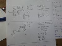
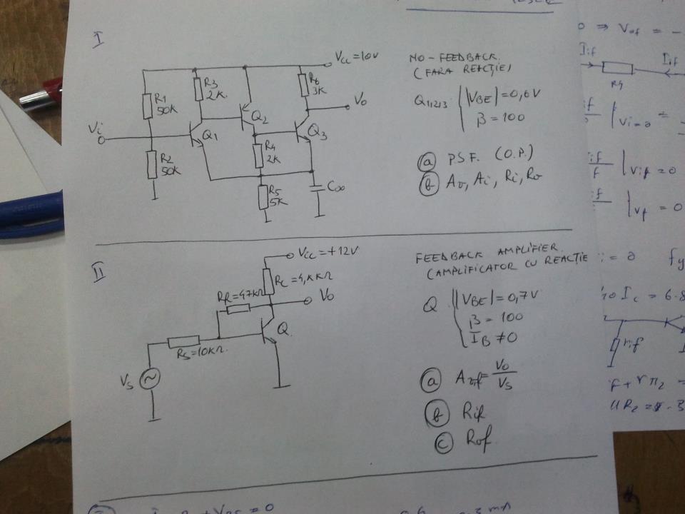
1) The first one is an amplifier without feedback and I need to calculate the static operating point for all 3 transistors, the voltage amplification, the current amplificator and the input and output resistances.
2) The voltage amplification and the input and output resistances for a feedback amplifier.
I would really appreciate help for 2 problems that I really can't figure out.
1) The first one is an amplifier without feedback and I need to calculate the static operating point for all 3 transistors, the voltage amplification, the current amplificator and the input and output resistances.
2) The voltage amplification and the input and output resistances for a feedback amplifier.
Last edited: