Continue to Site

Welcome to EDAboard.com

Welcome to our site! EDAboard.com is an international Electronics Discussion Forum focused on EDA software, circuits, schematics, books, theory, papers, asic, pld, 8051, DSP, Network, RF, Analog Design, PCB, Service Manuals... and a whole lot more! To participate you need to register. Registration is free. Click here to register now.

Cascaded 555s behaving strangely

abuhafss

Full Member level 2
Joined
Aug 8, 2010
Messages
142
Helped
1
Reputation
2
Reaction score
0
Trophy points
1,296
Activity points
2,383
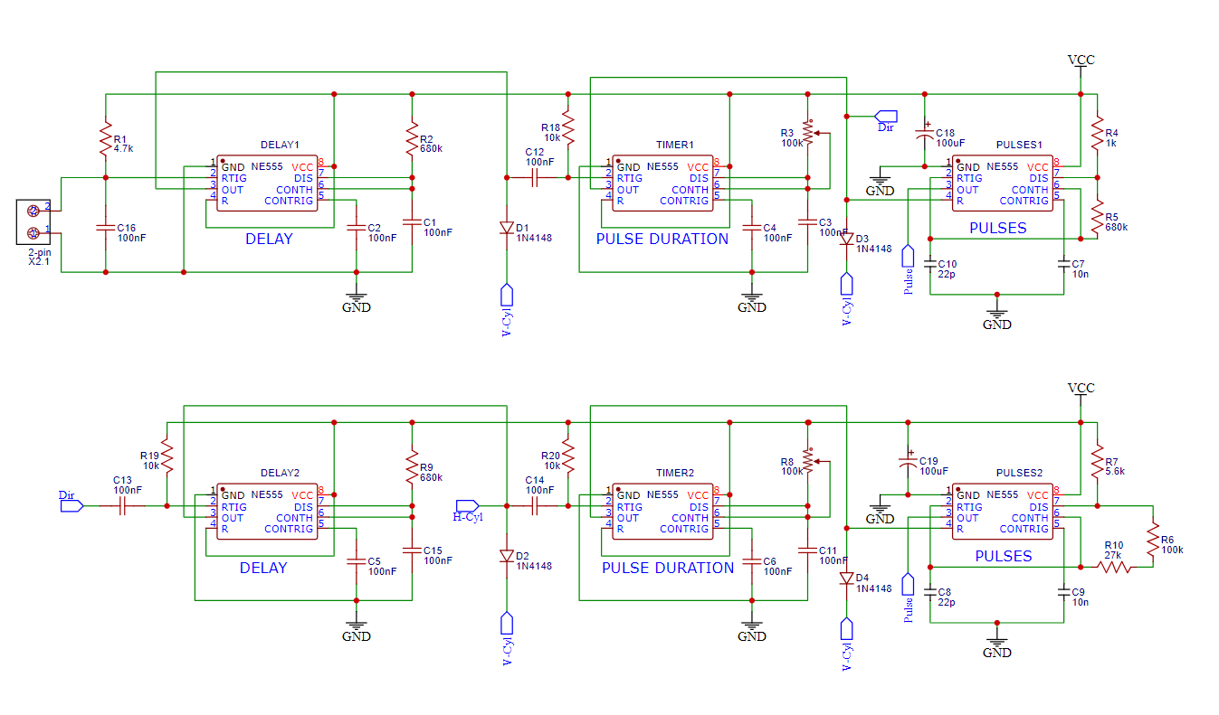
Here is a schematic containing a few cascaded 555 chips.
1716121035573.png
The flow of the circuit is as follows:

a) When a push button across C16 is pressed, DELAY1 (555 configured as monostable) would cause delay depending upon the values of R2 + C1.
b) After the delay, TIMER1 (555 configured as monostable) gets triggered thru C12. Then TIMER1 would power on PULSES1 (555 configured as astable) for a duration depending upon the values of R3 + C3.
c) PULSES1 would generate pulses depending upon the values of R4 + R5 + C10.
d) When the TIMER1 duration is completed, PULSES1 gets off and DELAY2 is triggered thru C13.
The lower 3 x 555 are almost copy of the upper 3 x 555.
e) DELAY2 causes a delay then triggers TIMER2.
f) TIMER2 switches on PULSES2, which generates pulses.

The outputs are V-Cyl, Dir, Pulse and H-Cyl, each have an LED connected thru a current limiting resistor.

Theoretically the circuit seems OK, simulation is also OK. But physically, I am facing some problems:

a) If TIMER2 is present, there will be no output at DELAY2. (H-Cyl LED doesn't light up).
b) if TIMER2 is removed, DELAY2 will give output and H-Cyl LED would light up. Interestingly, PULSES2 also generates pulses though without TIMER2.
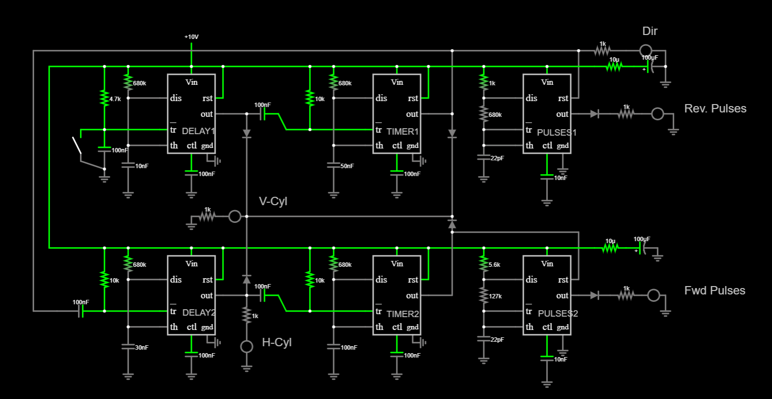
1716120794267.png

The values of the timing components, in the simulator are changed for speeding up the results.
 
Be careful with supply decoupling, NE555s pulse current at the Vin pin as they change state.
However, there is a potential design flaw repeated three times. Look at the 100nF capacitors at the output of the first, third and fourth ICs, when the output of the NE555 is low, they charge to 10V through the following 10K pull-up resistor. When the output of a 555 goes high, it lifts the driven side of the capacitor high so momentarily the 10K side rises to about 20V and could damage the following IC or cause operational problems.

I have seen a similar system in a commercial tape deck I was asked to investigate. It worked for a while then died with ICs with holes blown through their tops! Not my design I promise.

Brian.
 
Here is a schematic containing a few cascaded 555 chips.
View attachment 190887The flow of the circuit is as follows:

a) When a push button across C16 is pressed, DELAY1 (555 configured as monostable) would cause delay depending upon the values of R2 + C1.
b) After the delay, TIMER1 (555 configured as monostable) gets triggered thru C12. Then TIMER1 would power on PULSES1 (555 configured as astable) for a duration depending upon the values of R3 + C3.
c) PULSES1 would generate pulses depending upon the values of R4 + R5 + C10.
d) When the TIMER1 duration is completed, PULSES1 gets off and DELAY2 is triggered thru C13.
The lower 3 x 555 are almost copy of the upper 3 x 555.
e) DELAY2 causes a delay then triggers TIMER2.
f) TIMER2 switches on PULSES2, which generates pulses.

The outputs are V-Cyl, Dir, Pulse and H-Cyl, each have an LED connected thru a current limiting resistor.

Theoretically the circuit seems OK, simulation is also OK. But physically, I am facing some problems:

a) If TIMER2 is present, there will be no output at DELAY2. (H-Cyl LED doesn't light up).
b) if TIMER2 is removed, DELAY2 will give output and H-Cyl LED would light up. Interestingly, PULSES2 also generates pulses though without TIMER2.

View attachment 190886
The values of the timing components, in the simulator are changed for speeding up the results.
I see your problems but you do not have a question or an expectation not being met.
Share the sim. shortcut link and your expectation, s'il vous plais.
 
Just a though but generating various triggered pulse trains can all be done
with 1 part, quite easily, and with much more accurate timing :


Regards, Dana.
 
Be careful with supply decoupling, NE555s pulse current at the Vin pin as they change state.
However, there is a potential design flaw repeated three times. Look at the 100nF capacitors at the output of the first, third and fourth ICs, when the output of the NE555 is low, they charge to 10V through the following 10K pull-up resistor. When the output of a 555 goes high, it lifts the driven side of the capacitor high so momentarily the 10K side rises to about 20V and could damage the following IC or cause operational problems.

I have seen a similar system in a commercial tape deck I was asked to investigate. It worked for a while then died with ICs with holes blown through their tops! Not my design I promise.

Brian.
OK. Then what would be the best way to overcome that issue. Tying up a zener at the 10K side would do?
 
For Future reference this can be done easily, with more accurate timing :

1716127054542.png


Regards, Dana.
 
I see your problems but you do not have a question or an expectation not being met.
Share the sim. shortcut link and your expectation, s'il vous plais.
I thought, that was obvious, I simply want the circuit to perform without those problems.
--- Updated ---

For Future reference this can be done easily, with more accurate timing :

View attachment 190901


Regards, Dana.
Thank you Dana.
Yes, I know ATTiny85 can be used instead and I have used it number of times. However, the current project is limited to 555s.
--- Updated ---

Share the sim. shortcut link and your expectation, s'il vous plais.
The shortcut link is very lengthy.
Instead, I have copied the text for the circuit and saved in the attached file.
You may copy/paste the text into Paul Falstad's simulator.
 

Attachments

  • 555 circuit.txt
    4.9 KB · Views: 25
Last edited:
Hi,

I´m doing electronics for more then 3 decades. At the very beginning I had the opinion th NE555 was outdated.
Seems my opinion is wrong. It cannot be killed.

Klaus
 
Replies above are helpful...
My experience: More than once I've hooked up a hardware 555 to output a pulse train. At first I could not see any 'idle' time until I fiddled with oscilloscope settings to focus on that part of the waveform. It's like the duty cycle was 99.9%.

I believe it has to do with pin #5 and what voltage it adopts at the upper terminal of the capacitor (usually seen in schematics using a 555). I've applied a range of volt levels to pin 5 and seen the duty cycle respond. Also hi and low times.
 
I believe it has to do with pin #5 and what voltage it adopts at the upper terminal of the capacitor (usually seen in schematics using a 555). I've applied a range of volt levels to pin 5 and seen the duty cycle respond. Also hi and low times.
When TIMER2 is present, the voltage at pin 5 of DELAY2 is 4.78. No change when button is pressed.
Without TIMER2, the voltage at pin 5 of DELAY2 is 4.90. When button is pressed it changes to 4.80.
--- Updated ---

Using 555s at all isn't a good solution but the fix for the over-voltage problem is to add a diode across the 10K pull-up resistors so it dumps excess to the supply rail.

Brian.
I added a diode across R18, R19 and R20. No change in performance, the problem is still there.
Even, I lowered the value of C14 to 10nF. No change.
 
Last edited:
When TIMER2 is present, the voltage at pin 5 of DELAY2 is 4.78. No change when button is pressed.
Without TIMER2, the voltage at pin 5 of DELAY2 is 4.90. When button is pressed it changes to 4.80.

These readings are about half of a 10v supply. In that case waveforms are recognizable, no problem.
 
1716290558442.png

Pin 2 of DELAY2, when TIMER2 is present.

1716290756020.png

Pin 2 of DELAY2 when TIMER2 is removed.

These might give some clue for the abnormal performance.
 

LaTeX Commands Quick-Menu:

Similar threads

Part and Inventory Search

Welcome to EDABoard.com

Sponsor

Back
Top