Continue to Site

Welcome to EDAboard.com

Welcome to our site! EDAboard.com is an international Electronics Discussion Forum focused on EDA software, circuits, schematics, books, theory, papers, asic, pld, 8051, DSP, Network, RF, Analog Design, PCB, Service Manuals... and a whole lot more! To participate you need to register. Registration is free. Click here to register now.

BD437g Transistor Checker Circuit

Status
Not open for further replies.

AllenPitts

Newbie level 4
Joined
Jan 30, 2021
Messages
7
Helped
0
Reputation
0
Reaction score
0
Trophy points
1
Activity points
107
Hello EDABoard forum,

Working on system that will takes the 5v output from an Arduino and turns on eighteen LEDs.
So using a BD437g transistor because more current is needed than the Uno will output.

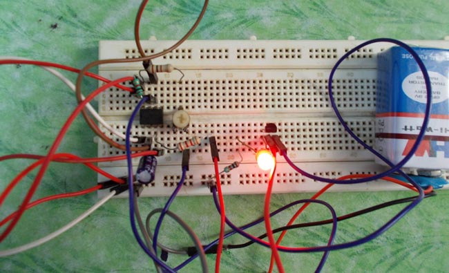
Having trouble working and understanding how the BD437g so a simple circuit was created
Transistor_Checker_One_210130.gif

This circuit does not work.
It is surmised that ...Checker One doe not work because there is no
positive voltage to make the LED glow.

So a second circuit was designed and built:
Transistor_Checker_Two_210130.gif


Cant get this circuit to work either.

Perhaps the problem with ....Checker Two is both grounds are connected to the Emitter of the Q1.
But if only, say, the voltage source 1 is connected to the Q1 emitter where does the ground for the Source 2
go?

Is there a better way to approach the circuit. Have searched on line for a simple transistor
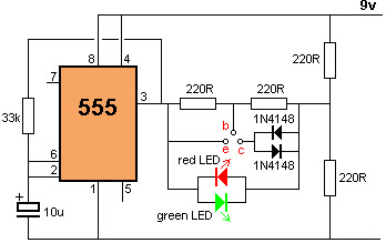
circuit to better understand how they work. Have found several circuits that use a 555 timer
as a transistor checker.


Hoped to build a very simple circuit that would demonstrate how the
the BD437g. Is there a simple way to refactor one of these circuits to
make the transistor turn the LED on?

Thanks.

Allen
 

D1 not reversed in circuit, or source2 ? The two circuits dont have the diode in
the same polarity, circuit with 12V source2 is correct.

You check LED with just the 12V and 430 ohms all in series ?

The 10K in base circuit a tad high. Normally you want a forced beta of 10. That is
Ib = Ic / 10.


So pick a target LED current, then

So Ic = Iled = (12 - Vcesat - Vled) / Rled or Rled = (12 - Vcesat - Vled) / Iled (Rled is R in series with led)

Vcesat and Vled come from their datasheets at the target current you want.

Then Rbase = ( 5 - Vbe ) / (Iled / 10 )


Regards, Dana.
 
Last edited:

Hi,

At first I was confused with the battery symbols and the "+".

But there is "NEG" and "POS".
Be sure you used "NEG" as "-" minus and
"POS" as "+" plus

You may use free circuit simulation software.
If there still are problems show a photo of your circuit.


Klaus
 

Hi,

A transistor, a few resistors, a pushbutton (or control signal) and an LED is good enough for a 'does it work' circuit.

Connect both supply grounds together, otherwise neither circuit/supply has a common reference - look for 'star ground' and read a bit about it. Two versions: One with only a 5V supply, one with 5V for control signal and 12V for power to the LEDs. The pushbutton would be the control signal from your Arduino. If this is just to test a batch of transistors and the only interest is if an LED lights up or not briefly, iC/iB can easily be 10 or even 50, regarding R3:R1 (R6:R4) ratio, and I'd configure it for 5mA into the LEDs. The LEDs in the simulation are 1.7V LEDs, btw. The capacitor is to soften the turn on and off of ther BJT.

EDABOARD BD437G TESTER V3 BOTH TOGETHER.JPG
 

Hello Danadakk, Klausst, d123 and the ED Board forum,

Danandak:
...Checker One does have LED reversed. The LED in ....Checker Two has the polarity of the LED correct but the circuit does not work.
So Ic = Iled = (12 - Vcesat - Vled) / Rled or Rled = (12 - Vcesat - Vled) / Iled (Rled is R in series with led)
Not sure what this means. I am a bit of a newb, so I know Ohms Law and some other concepts but that is a bit over my head. Is there
a knowledge base where I could get the knowledge to figure that out?

d123:
I may have mislead you, because of the schematic symbols used, into thinking that batteries were being used, but regulated AC/DC converters (wall warts) are used. Although not sure there is a difference between batteries and wall warts since they are both voltage sources with grounds. (Maybe the internal resistance called out in the second schematic from post # 4 is different in comparing AC/DC converters to batteries.)

Did not grasp the first schematic but could get an idea about how the second schematic is designed to work.
Even so there were elements of the second schematic that were not understood so the schematic was redrawn.
BD437g_Circuit Schematic_210131.jpg


It is believed that this is a faithful redrawing of the second schematic in post #4

This is a photo of a breadboard of this schematic.
A pushbutton was not included because there was not one on hand and disconnecting
one of the jumpers can act as a switch. Also did not have 1.5k resistor so I put
a 1K and a 470 resistors in series.

BD437g_Circuit_breadboard_photo_210131.jpg


It maybe a bit hard to see the connections in the photo so a Fritz diagram was done:

Transister_Checker_210131.jpg


No luck getting the circuit to operate.
Tried substituting a nine volt for the five volt source but no joy.
Also though maybe the LED had been reversed but tried it both ways,

Has the second schematic in post #4 been not replicated accurately?

Thanks.

Allen
 

In your circuit your 470 Base to ground will keep Q1 off.

Swap R 1 and R2, with R1 now 470 ohms connect it to + 5 LED should come on.

The calculations I made are basic circuit analysis. There is tons of basics
on youtube that can walk you thru this.

Essentially the sum of voltage drops around a loop = 0, and the sum of currents
entering and leaving a node = 0.


Regards, Dana.
 

An explanation may help. Ignore the connection of the transistor base
for a moment.

R1 and R2 form a V divider, Vjunction = (5V * R2) / ( R 1 + R2). So for the values
and locations you had Vjunc = ( 5 * .47 ) / ( 10 + .47 ) r values in K ohms
So Vjunc = .22 V

Now we connect base of transistor to that junction, but it wants to turn on around
~ .7V for a silicon bipolar transistor. So it never got turned on. Here is a graph of
Vbe and Ic, current in the collector, same current in your LED, for a "typical" NPN
transistor -

1612141024627.png


So your voltage divider was prohibiting the transistor from turning on.

But if you swap their values then Vjunction = (5V * R2) / ( R 1 + R2)
= ( 5 * 10 ) / ( 10 + .47) = ~ 4.8 V. But at .7 V that Base Emitter junction
turns on and as you can see from the graph it does not want to change
its Vbe much so acts as a sort of clamp in the base circuit. But its turning
on the transistor hard.

Here is a graph of base current versus its Vbe, as you can see once it
turns on it does not want its Vbe to change much. Thats the nonlinear
behavior of a basic diode junction.

1612141664479.png
i

Keep in mind in a NPN Ic =~ Beta x Ibase, so in this graph if 80 uA was
shoved into the base and Beta was 100 then the collector current would
be 8 mA.

So we want the transistor to operat as a switch, basically to make Vce as
low as possible. We can do that by forcing much more current into the base,
rule of thump is Ib = Ic / 10. As you can see in this graph the sat region of oper-
ation, cross hatched area (vertical cross hatched area) , shows Vce quite low,
base current quite high relative to I collector.

Note Ib/10 is called "forced beta" in the industry.

1612142156979.png


The region out of the cross hatched areas is the linear operation of the transistor when
we use it to amplify signals. Where its beta become important. A whole lot of other con-
siderations come into play here.


Regards, Dana.
 
Last edited:

Hi,

The schematic of post#5 has some mistakes:
* C1 is drawn the wrong way round
* +5V, GND and +12V are wired to the same node ... leading to short circuit 5V as well as 12V supplies.

Klaus
 

Hi,

Much has already been corrected. Your schematic does not reflect the version drawn of the breadboard and is not the same as the second version I drew. Breadboards can be confusting at first. Capacitor polarity, looking at the parallel lines of the symbol (when the capacitor is a polarized one): curvy line = most negative potential (potential = voltage) connection, straight line = most positive potential connection - the stripe on electrolytic capacitors shows you which lead to connect to ground/most negative potential in the circuit. Your polarized capacitor symbol is 'happy'/'smiling', it should be 'unhappy'. You can damage electrolytic capacitors if you do not observe the correct polarity in real life and make Tantalum capacitors set on fire. Your seemingly ceramic capacitor (MLCC) is presumably not polarized so it can go either way without problems.

As already said, swap R1 and R2 over. The resistor that goes to ground (to hold the transistor to a defined potential and so make it stay off when there is no input/control signal) should be (much) larger than the resistor that goes in series with the base and is there to create the base current.

You have connected the capacitor in parallel to the base resistor. No idea why... The capacitor should have one lead connected to the junction of the base resistor and to the BJT base and its other lead connected to ground (the same as R2 is connected in my and in your schematic). Move the capacitor lead connected to the transistor base and connect that capacitor lead to ground.

Your supplies are wired correctly, btw, assuming that red means positive lead and black means negative lead of each supply.

It's easy to get transistor connections wrong, especially on breadboards - and, sometimes the datasheet pinout shows the device from the top but you think it's from the bottom. Just so you know.

1.5k was a fairly arbitrary choice to keep the LED current at the arbitrary choice of around 7mA, so I wouldn't worry about that. As you are using a wall wart, the current is unlimited forever and ever - unlike with a battery - but even so, just to see if the LED lights up or not, I like to be economical with current (you never have enough of the stuff where battery-powered circuits are concerned), especially in this age of insincere words about urgent climate action (buy the feelgood slogan, if not the readily-available tools to remedy the issues we face ;)) and with 1mA to 2mA you will definitely see if the LED is illuminated or not/on or off, that could be a 4.7k or 5.1k as the collector/LED resistor.

Presumably it's working now, hopefully. Best of luck.
 

The breadboard has the base of the transistor connected to ground. Then the transistor will never turn on.
Breadboards are a tangled mess of wires (antennas for interference) all over the place, lots of stray capacitance between the wires and rows of contacts and intermittent connections.
 

Normally when you use these breadboards the Red is for + supply, the blue for ground.
Additionally you do not loop a wire from red at bottom to blue at top of board. You want to be
consistent, so when you plug something into red its ALWAYS same buss weather you plug into
top red buss or bottom red buss.

Same comments apply to ground, blue.

Just a thought.

Regards, Dana.
 

Hello Danadakk, D123, AudioGuru, KlaussT and the EDABoard,

Thanks for all the excellent feedback.

Got the LED to glow using this configuration. (AudioGuru, sorry breadboards are disliked, but don't know of another way
to prove electrical theory before committing to a PCB.)

Transister_Checker_210131_b.jpg


First tried exchanging the values of resistors R1 and R2 but that did not work.

Then began to think about the comment by Danadakk at post #6 and AudioGuru
at post # 7 and removed the jumper between the transistor base and ground.
That is, removed the jumper between nodes 14 and 15. Bingo. The LED came on.

Still curious about how things developed.
We started with this schematic
Schematic_210130_from_Post_#_4.jpg


Granted I am the newb here but I thought that this schematic (210130 from Post #4)
was equivalent to the one in post#5
BD437g_Circuit Schematic_210131.jpg


In both R1 is connected in series to the 5v supply and connected R2 & C1 joined to the ground
and the Q1 base.

I think what we have in the revised breadboard Fritz (...Revised 210201') that works is:
BD437g_Circuit Schematic_210201.jpg


So is Schematic 210130 from Post #4 more like BD437g Transistor Circuit Schematic or more like
BD437g Transistor Circuit Schematic, Revised 210102... ?

Thanks again for you patience and courtesy in putting up with my newbness.
It is written: 'The recognition of ignorance is the beginning of knowledge.'

Allen
 

Hi,

* Still 5V is short circuited to GND
* 12V, too.

If you don't correct the issues, it makes non sense for further discussion.

It is similar to a car with no motor, but the driving shaft welded to prevent movement.

Klaus
 

Hi,

Great to hear that it is working now. Good for you.

Klaus is right, in the schematics (not the breadboard pictures) you keep connecting the positive of the power supplies to their grounds with a wire - that would be a short-circuit in real life. Take care with what you do and draw - somebody else with less experience might copy that mistake.

To save time, and pictures can be faster than words, I have redrawn your working version for a couple of reasons. Look for pull-down and pull-up resistors to understand why it would be preferable for R2 (and C1) to be connected to ground and not in series with the transistor base.

If we do the quick ball-park figure sums [and we'll ignore the voltage divider effect of 5V * (R2/(R1 + R2)) as it would only change the voltage by about 300mV]:

5V - Q1 Vbe = 4.3V
4.3V/470 Ohms = 9mA
4.3V/10,470 Ohms = 0.41mA

Big difference in the base current there when you put R2 in series with R1, instead of to ground where it is supposed to be. 9mA base current is overkill to light up an LED with only a few mA collector current. Oddly, the 410uA (0.41mA) goes well with iC/iB = 10 for a collector resistor of 1.5k, in a rough and ready way.

BD437G corrected schematic.jpg
 

Status
Not open for further replies.

Part and Inventory Search

Welcome to EDABoard.com

Sponsor

Back
Top