saqib.shah06
Junior Member level 2
Hi everyone,
I had a question regarding the biasing of my Deep N well guard ring.
I am using a deep N-well to isolate a low noise OTA in my ADC. The chip also has a analog section (not in DNW), and a noisy digital section. I have been able to figure out the biasing for the analog and digital sections, but I am having some issues with the deep N well analog section , I am using the following strategy for all the guard rings. Any criticisms would be welcome.
1. Digital section : A Digital VDD and GND rail with dedicated pads. Also, a p-tap guard ring surrounding the digital block with a separate VDD pad.
2. Analog section : An analog VDD and GND rail with separate pads. Again, a p-tap guard ring surrounding the analog block with a separate VDD pad (lets call is GR_AVDD).
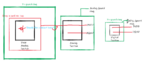
3. Deep N well (DNW) analog section :
There is a p well guard ring surrounding the DNW section that connects to the GR_AVDD pad. The DNW also has N well taps around its edges that go to the analog VDD.
For the Deep N well section, the NMOS transistors have a separate ground and bulk connection that that goes to a dedicated pad.
Here are my questions:
1. I cant figure out the biasing for the PMOS transistors inside the DNW. Should the body contacts of these be connected directed to the DNW guard ring or should they be connected to a separate pad?
2. Is it proper to connect the N+ DNW contacts to analog VDD or will this introduce additional noise into the VDD rail?
I have attached a figure to give you a rough sketch of what I am doing.
Thanks for any inputs.
I had a question regarding the biasing of my Deep N well guard ring.
I am using a deep N-well to isolate a low noise OTA in my ADC. The chip also has a analog section (not in DNW), and a noisy digital section. I have been able to figure out the biasing for the analog and digital sections, but I am having some issues with the deep N well analog section , I am using the following strategy for all the guard rings. Any criticisms would be welcome.
1. Digital section : A Digital VDD and GND rail with dedicated pads. Also, a p-tap guard ring surrounding the digital block with a separate VDD pad.
2. Analog section : An analog VDD and GND rail with separate pads. Again, a p-tap guard ring surrounding the analog block with a separate VDD pad (lets call is GR_AVDD).
3. Deep N well (DNW) analog section :
There is a p well guard ring surrounding the DNW section that connects to the GR_AVDD pad. The DNW also has N well taps around its edges that go to the analog VDD.
For the Deep N well section, the NMOS transistors have a separate ground and bulk connection that that goes to a dedicated pad.
Here are my questions:
1. I cant figure out the biasing for the PMOS transistors inside the DNW. Should the body contacts of these be connected directed to the DNW guard ring or should they be connected to a separate pad?
2. Is it proper to connect the N+ DNW contacts to analog VDD or will this introduce additional noise into the VDD rail?
I have attached a figure to give you a rough sketch of what I am doing.
Thanks for any inputs.

")